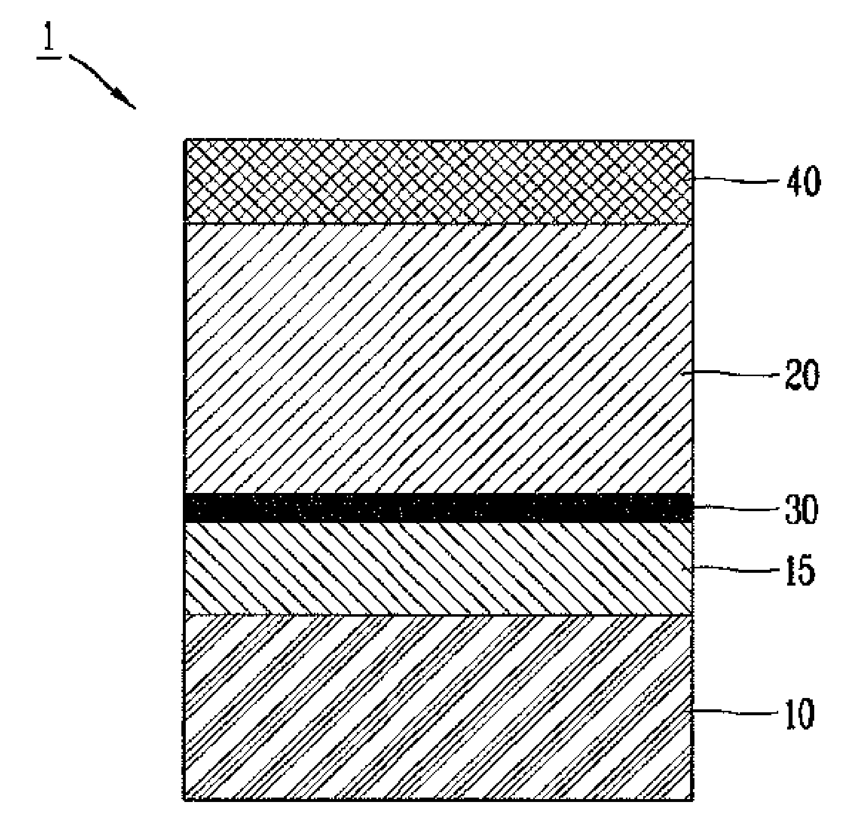
Silicon thin film anode for lithium secondary battery and preparation method thereof
a lithium secondary battery and thin film anode technology, which is applied in the field of lithium secondary battery thin film anode and a preparation method thereof, can solve the problems of complicated conventional structure and preparation methods, and achieve the effect of enhancing capacity and cycle characteristics of the battery
- Summary
- Abstract
- Description
- Claims
- Application Information
AI Technical Summary
Benefits of technology
Problems solved by technology
Method used
Image
Examples
example 1
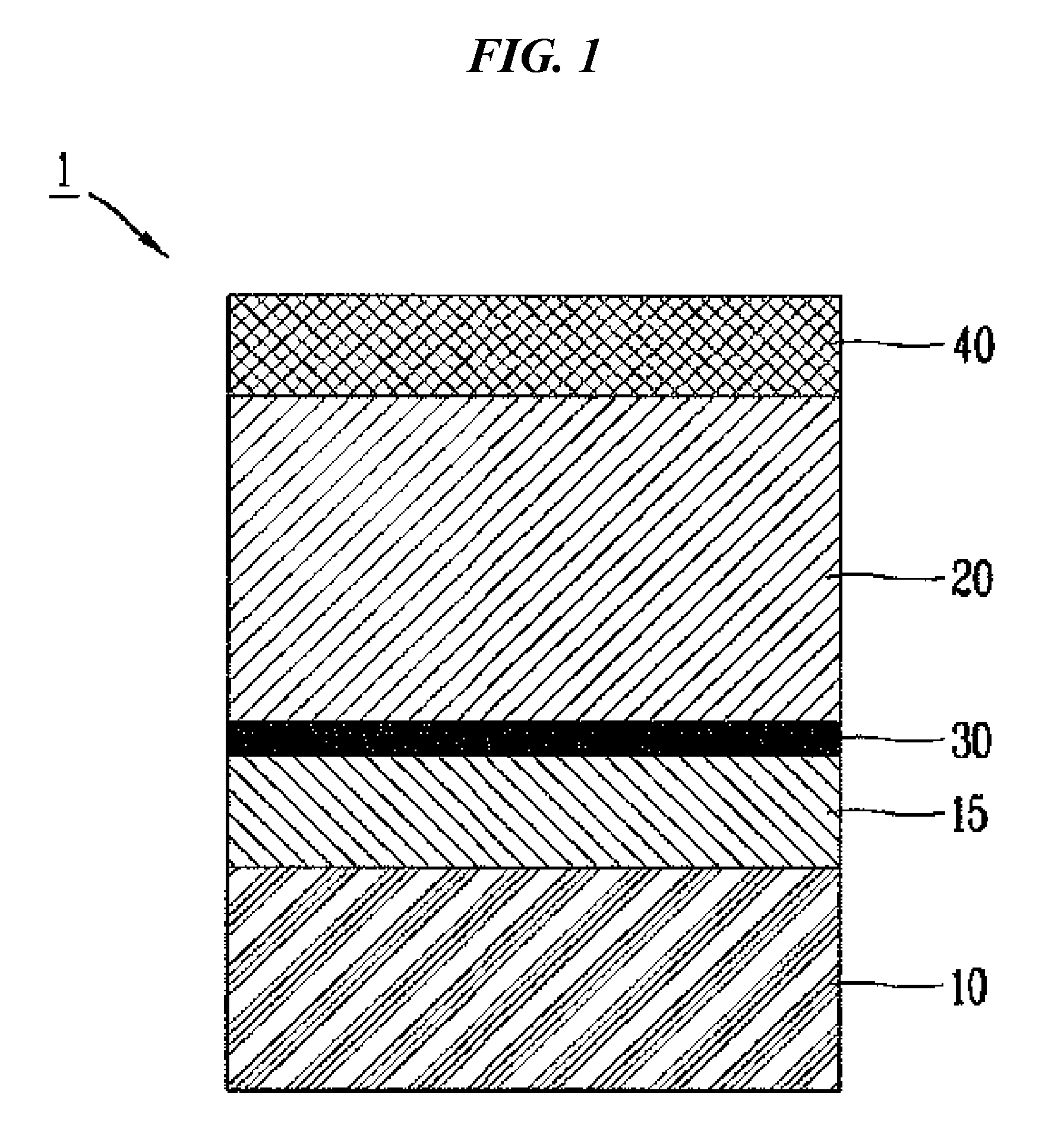
[0071]In the example 1, an anode active material layer was formed of only a silicon thin film, and the metallic buffer layer of FIG. 1 was not formed.
[0072]Firstly, a collector formed of a copper foil was prepared. Then, an anode active material layer (silicon thin film) was deposited on the collector by an RF magnetron sputtering process using a silicon target having a purity of 99.9%. Here, the silicon thin film was deposited to have a thickness of 500 nm. The thickness of the silicon thin film was observed by using an atomic force microscope (AFM) or an alpha step surface profiler, etc. In order to enhance an interface characteristic between deposited layers, the deposited thin film anode underwent an annealing process in an argon atmosphere by using a rapid thermal analyzer (RTA). The annealing process was performed for 20 minutes at a temperature of 400° C. having initially raised for 5 minutes. Then, the temperature of 400° C. drastically dropped to 25° C. Next, the annealing ...
example 2
[0077]In the example 2, a metallic buffer layer was formed, and an anode active material layer was formed of only a silicon thin film.
[0078]Firstly, a metallic buffer layer (titanium thin film layer) having a thickness of 50 nm was deposited on a collector by an RF magnetron sputtering process using a titanium target having a purity of 99.9%. Then, an anode active material layer (silicon thin film) was deposited with a thickness of 500 nm on the metallic buffer layer. The deposited silicon thin film anode underwent an annealing process and a carbon coating process in the same manner as the example 1. Then, in order to observe a performance and cycle characteristics of the prepared silicon thin film anode, a half cell assembly is performed in the same manner as the example 1.
example 3
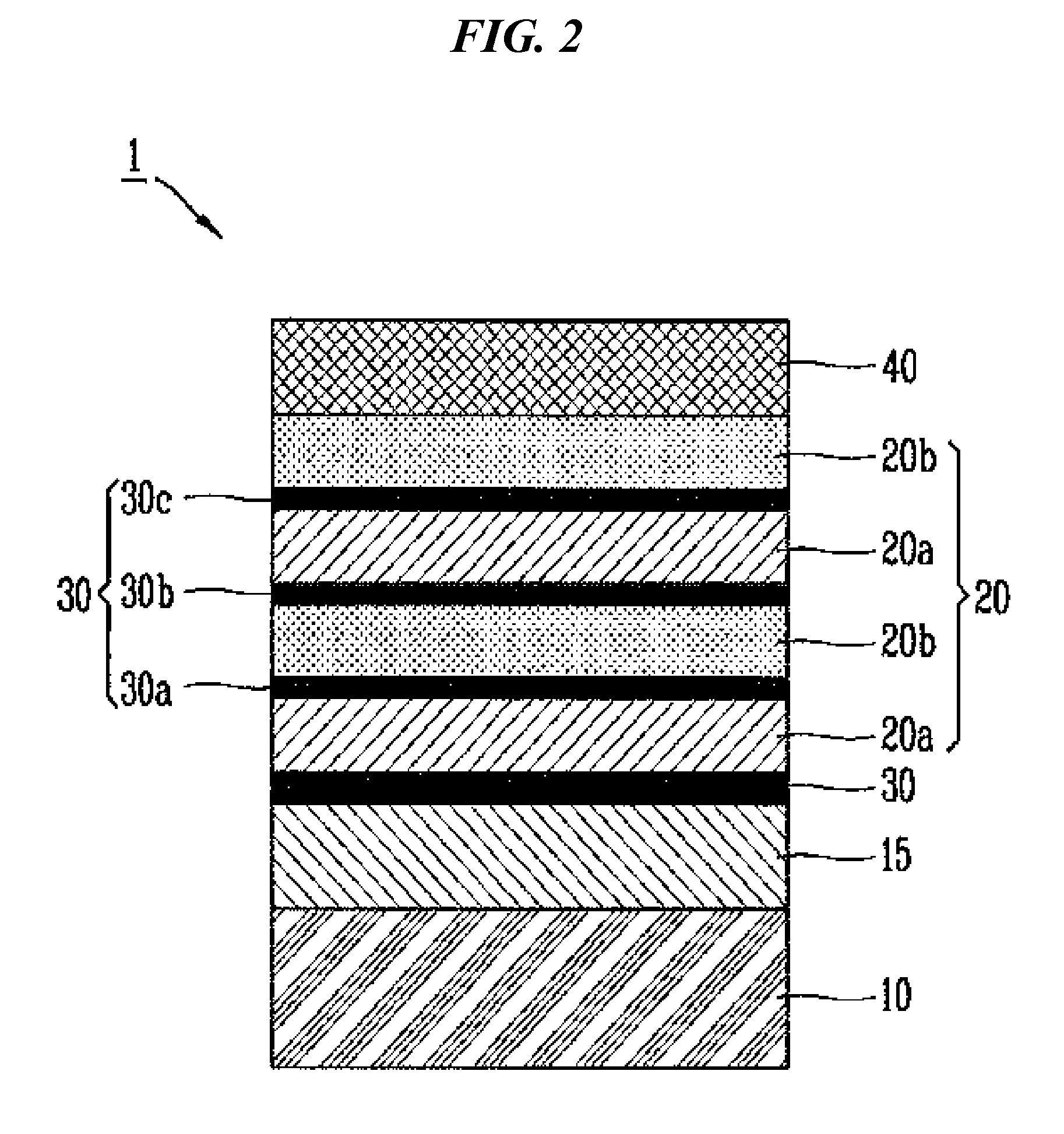
[0083]In the example 3, a metallic buffer layer was not formed, and an anode active material layer was formed of a silicon-metal single layer to undergo an annealing process.
[0084]More concretely, silicon and titanium were simultaneously deposited on a collector formed of copper by using a silicon target and a titanium target, thereby depositing an anode active material layer (silicon-metal single layer) having a thickness of 500 nm. Then, the deposited silicon thin film anode underwent an annealing process and a carbon coating process in the same manner as the example 1, thereby performing a half cell assembly. When the anode active material layer was formed of a silicon-metal single layer, a metallic component was distributed into a silicon thin film uniformly enough to approximately correspond to an alloy. Accordingly, conductivity lowering due to volume change of the silicon thin film was minimized. That is, even if the silicon thin film was broken, a conductivity of the silicon...
PUM
| Property | Measurement | Unit |
|---|---|---|
| Thickness | aaaaa | aaaaa |
| Thickness | aaaaa | aaaaa |
| Thickness | aaaaa | aaaaa |
Abstract
Description
Claims
Application Information
 - R&D
- Intellectual Property
- Life Sciences
- Materials
- Tech Scout
- Unparalleled Data Quality
- Higher Quality Content
- 60% Fewer Hallucinations
Browse by: Latest US Patents, China's latest patents, Technical Efficacy Thesaurus, Application Domain, Technology Topic, Popular Technical Reports.
© 2025 PatSnap. All rights reserved.Legal|Privacy policy|Modern Slavery Act Transparency Statement|Sitemap|About US| Contact US: help@patsnap.com


