
Flat panel display device and data processing method for video data

a display device and video data technology, applied in the field of flat panel display devices and data processing methods for video data, can solve the problems of increasing manufacturing costs, affecting the emi of an entire flat panel display device, and the circuit scale of the signal driver becomes too large, so as to improve the emi and improve the emi

Inactive Publication Date: 2009-01-15
RENESAS ELECTRONICS CORP
View PDF10 Cites 13 Cited by
  • Summary
  • Abstract
  • Description
  • Claims
  • Application Information

AI Technical Summary

Benefits of technology

The patent text discusses techniques for reducing electromagnetic interference (EMI) in flat panel display devices. The text describes methods for controlling data load timing and delay circuits to reduce peak currents and EMI. However, these techniques have limitations in terms of cost and dispersion of current peaks. The text also discusses the issue of EMI generated by a power supply and ground line used in common by multiple signal drivers. The text proposes a method for controlling delay circuits to address this issue. Overall, the patent text aims to provide a solution for reducing EMI in flat panel display devices.

Problems solved by technology

However, in accordance with the increase in the clock speed and the increase in the size of the display device, an influence of power supplies and an influence of deterioration in ground impedance have been significant.
However, for driving a large display panel by a single signal driver, the circuit scale of the signal driver becomes too large.
This results in increasing the manufacturing cost.
Further, wiring between the display panel and the signal driver becomes difficult due to the difference in their sizes.
However, the basic issue of the patent document 1 is the data load timing.
Therefore, with regard to the technique disclosed in the patent document 2, it is not possible to improve the excessiveness of the peak current of the recent flat panel display device and the EMI.
Further, the patent document 2 does not disclose a method for controlling a delay shorter than a system clock period, even though a shorter time than a transfer clock of video data is required for a delay time.
In general, it is difficult to provide a delay time difference that is stable and fine in controllability.
To control delay at this frequency leads to an increase in the cost (it is necessary to generate the timing by using PLL (Phase Locked Loop) in order to achieve a high precision and to expand a range of adjustment).
Thus, depending on the circuit, the range of adjustment may become narrow and sufficient dispersion of the current peaks cannot be done.
Therefore, depending on a combination of circuit products with different EMI characteristics, the EMI at a specific frequency may not be improved in mass-produced flat panel display devices.
Thus, it is considered that the third EMI issue, i.e., the EMI issue generated by a peak current value (dId / dt) of the power supply and the ground line used in common by the plurality of signal drivers is a dominant problem now.
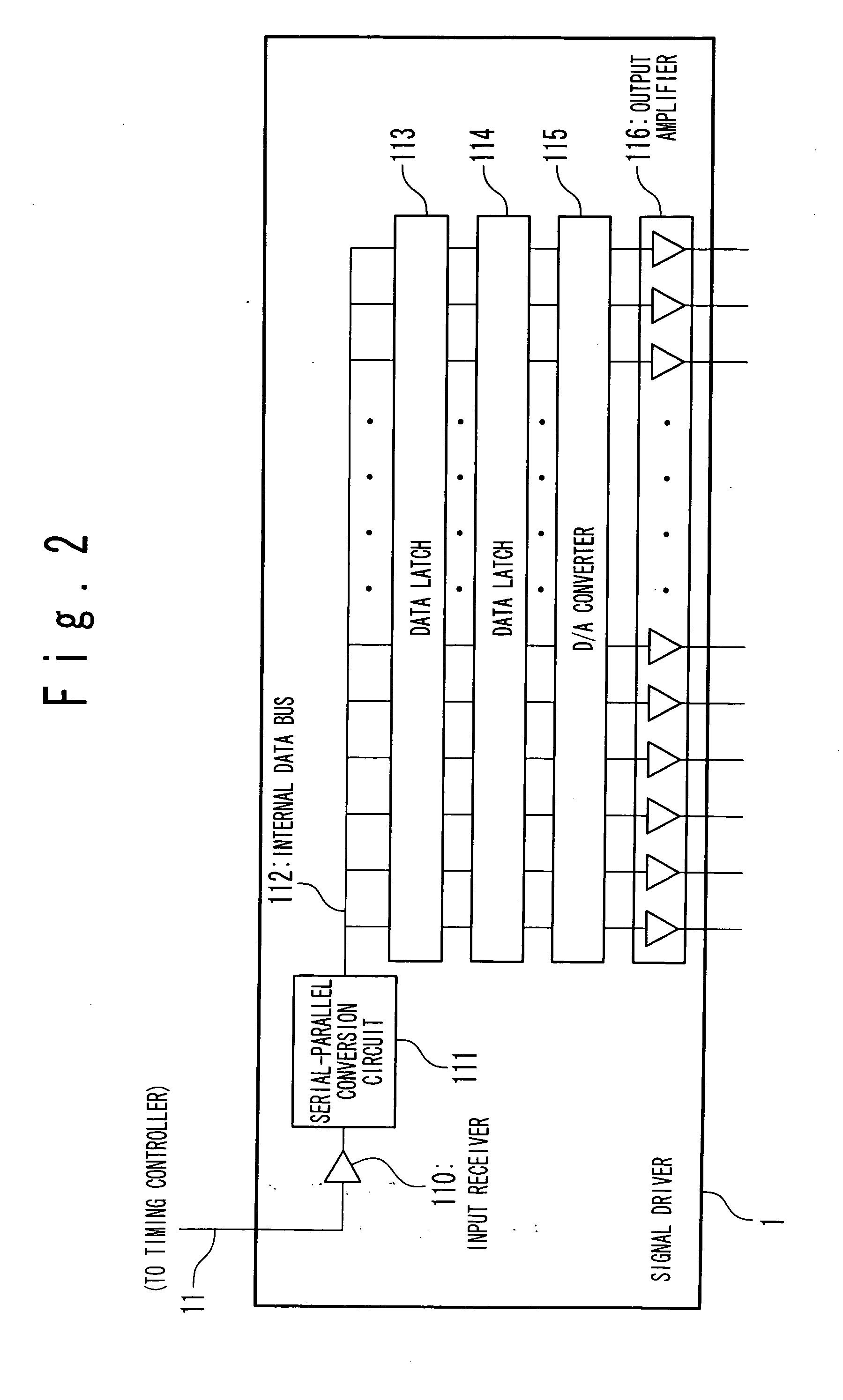
With this latch processing, a large amount of current is consumed in the signal driver 1 every time the one group of video data is switched.
As described, the peak currents generated in a plurality of signal drivers are generated at the same timing in the entire flat panel display device, thereby deteriorating EMI.

Method used


Image

  • Flat panel display device and data processing method for video data
  • Flat panel display device and data processing method for video data
  • Flat panel display device and data processing method for video data

Examples


Embodiment Construction

[0057]Hereinafter, a flat panel display device and a data processing method for the video data according to embodiments of the present invention will be described with reference to the attached drawings.

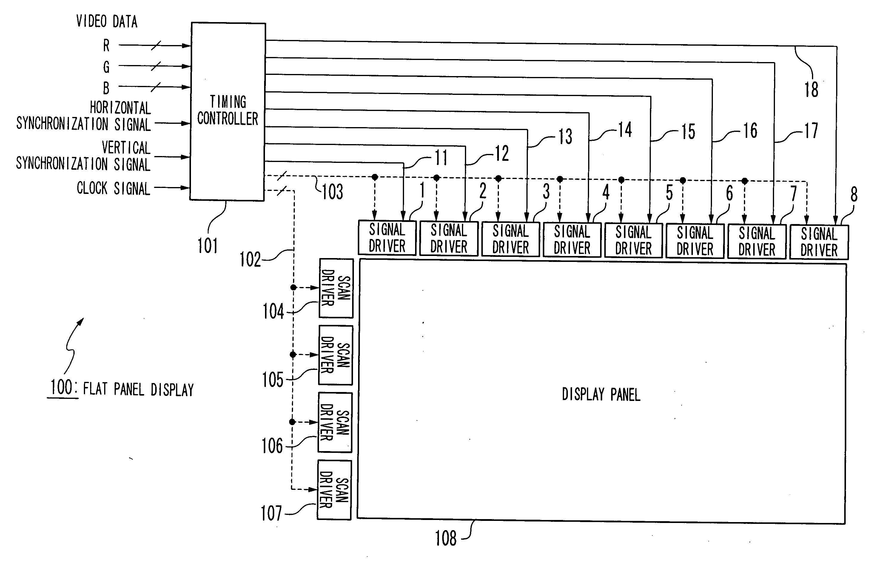
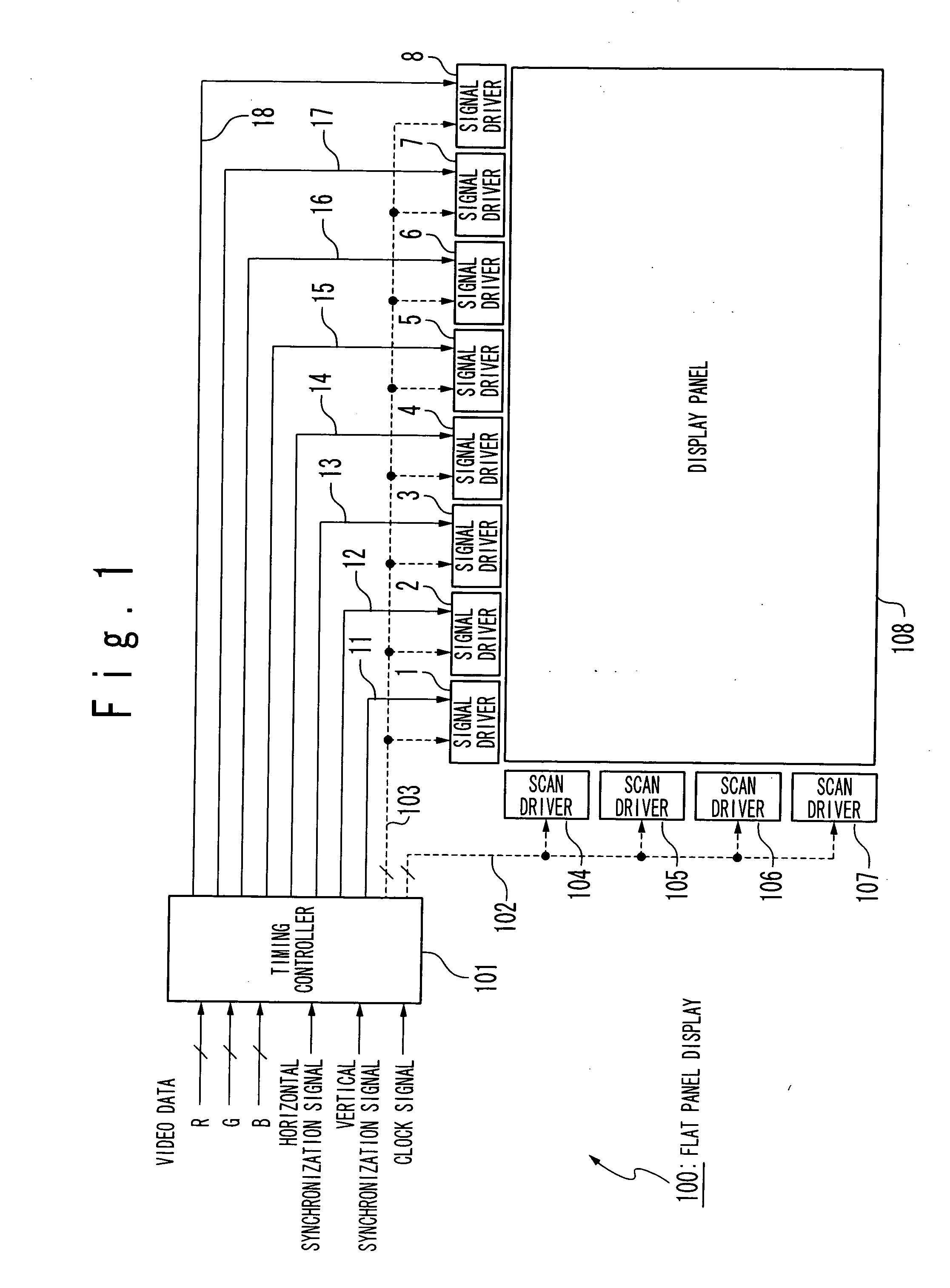
[0058](1) As shown in FIG. 1, a flat panel display device 100 is constituted roughly with a timing controller 101, signal drivers 1 to 8, scan drivers 104 to 107, a display panel 108, and data lines 11 to 18 which connect the timing controller 101 and the signal drivers 1 to 8. Among those, the timing controller 101, the signal drivers 1 to 8, and the data lines 11 to 18 are the factors that have large influences on the EMI.

[0059]In this embodiment, a point-to-point architecture and the small-amplitude serial data transfer architecture for transmitting signals between the timing controller 101 and the plurality of signal drivers 1 to 8 are employed so as to overcome the EMI issue caused due to the timing controller 101 and the EMI issue caused due to the data lines 11 to 18.

[0060]Fur...


PUM

PropertyMeasurementUnit
frequencyaaaaaaaaaa
peak currentsaaaaaaaaaa
current consumptionaaaaaaaaaa

Abstract

A flat panel display includes first and second signal drivers which drive a first and second group signal lines of a display panel in accordance with an input first and second group video data respectively. A controller controls a timing of sending the first group video data to the first signal driver via the first data line, and a timing of sending the second group video data to the second signal driver via the second data line. A delay time generating section shifts a relative timing between a timing at which the first signal driver receives the first group video data and a timing at which the second signal driver receives the second video data by a determined time. The problem of the deterioration of the EMI caused by synchronization of the peak currents respectively generated in signal drivers for driving a flat panel display can be suppressed.

Description

INCORPORATION BY REFERENCE[0001]This Patent Application is based on Japanese Patent Application No. 2007-179382. The disclosure of the Japanese Patent Application is incorporated herein by reference.BACKGROUND OF THE INVENTION[0002]1. Field of the Invention[0003]The present invention relates to a flat panel display device such as a liquid crystal display and a plasma display, and to a data processing method for video data supplied to the flat panel display device.[0004]2. Description of Related Art[0005]In accordance with an increase in sizes of flat-panel type display devices such as liquid crystal television sets, higher definition and smoother motion have been demanded. In order to satisfy those demands, video data of still wider band is required so that a clock speed of such device has been enhanced. However, in accordance with the increase in the clock speed and the increase in the size of the display device, an influence of power supplies and an influence of deterioration in g...

Claims


Application Information

Patent Timeline
Patent Type & Authority Applications(United States)
IPC IPC(8): G09G3/28G02F1/133G09G3/20G09G3/36
CPCG09G3/20G09G2310/027G09G2370/08G09G2330/06G09G2310/08
Inventor HORI, YOSHIHIKO
Owner RENESAS ELECTRONICS CORP
Learn More