Semiconductor memory device

a memory device and semiconductor technology, applied in the direction of information storage, static storage, digital storage, etc., can solve the problems of reducing performance, enlarge the area of the memory cell, and inability to perform data read/write in the memory cell, so as to prevent the decrease of data read speed and malfunction, and reduce the influence of such variations

Inactive Publication Date: 2008-12-25
NEC ELECTRONICS CORP
View PDF6 Cites 17 Cited by
  • Summary
  • Abstract
  • Description
  • Claims
  • Application Information

AI Technical Summary

Benefits of technology

[0029]The object of the circuit in Non-Patent Document 1 is stable operation of a memory cell, an improvement in static noise margin (static characteristics) and an improvement in access time. At the time of same-address access in the circuit configuration of Non-Patent Document 1, only the access transistors on the side of the A port are used, the access transistors on the side of the B port are not used and only the port on one side is used. That is, the circuit is advantageous in that there is no influence from port-to-port variation of the access transistors.
[0033]FIG. 27 illustrates the circuit configuration disclosed in Patent Document 1. The circuit of Patent Document 1 aims to shorten write time by short-circuiting the bit line of one port and the bit line of the second port in a case where the word lines of a memory cell are accessed simultaneously from both ports in a state in which one port is in the write state with respect to the memory cell.
[0034]When one port is in the write state with respect to a certain memory cell, the fact that the row addresses of both ports match each other is sensed by a sensing circuit 4. That is, when the word lines on the sides of both ports connected to the memory cell are both being accessed, the sensing circuit 4 outputs the low level as a sense signal Sd. In the period of time during which the sensing signal Sd is at the low level, a bit line BL in the write state and a bit line BL′ of the inverse port connected to the bit line B1 via transfer gates are short-circuited by a first shorting circuit 5. Accordingly, the transfer gates are connected in parallel and the combined resistance thereof becomes half the resistance of one transfer gate. As a result, the time needed for writing is shortened.
[0036]In Patent Document 2, there is disclosed a two-port SRAM in which a column switch is provided with A-port switches, B-port switches and inter-port switches. When it is detected that an A-port row address and a B-port row address match each other, all of the B-port switches are turned off, and an A-port bit line pair for a column selected according to A-port column decode signals is coupled to an A-port data line pair, while an A-port bit line pair for a column selected according to B-port column decode signals is coupled via the inter-port switch to a B-port data line pair. However, the two-port SRAM in Patent Document 2, is configured such that when it is detected that the A-port row address and the B-port row address match each other, the A-port word line and the B-port word line are not driven simultaneously but only the A-port word line is driven, thereby preventing decrease in data read speed and malfunctions.
[0037]It is therefore an object of the present invention to provide a semiconductor memory device in which even if there are variations in the ON currents of access transistors of different ports in a multiport cell, the influence of such variations is reduced.
[0049]The present invention is such that even if there are variations in the ON currents of access transistors of different ports, the influence of such variations can be reduced. The reason for this is that in the present invention, the arrangement is such that when the word lines of different ports are accessed simultaneously, the inter-port switches are turned on to render the bit lines of the different ports connected each other, thereby discharging the bit lines of the different ports uniformly.

Problems solved by technology

If a variation in transistor characteristics (a difference in ON current between transistors of the same size having identical capabilities) is too large, this can lead to malfunction, namely an inability to perform memory-cell data read / write, by way of example.
If operating speed, for example, is lowered in order to avoid a decline in yield and reliability due to malfunctions that accompany a variation in transistor characteristics, this can leads to lowering of performance.
If the size of the memory cell is made too large in order to suppress a variation in characteristics due to the shrinkage in transistor dimension, this enlarges the area of the memory cell.
Consequently, the difference potential is inadequate for a sense amplifier to operate stably.
That is, a malfunction occurs.
Thus, in a case where the same memory cell undergoes simultaneous access to ports A and B in a dual-port RAM, a malfunction such as erroneous sensing of data in the memory cell tends to be caused by a port-to-port variation in the ON currents of the transistors that access the memory cell.

Method used


Image

  • Semiconductor memory device
  • Semiconductor memory device
  • Semiconductor memory device

Examples


Embodiment Construction

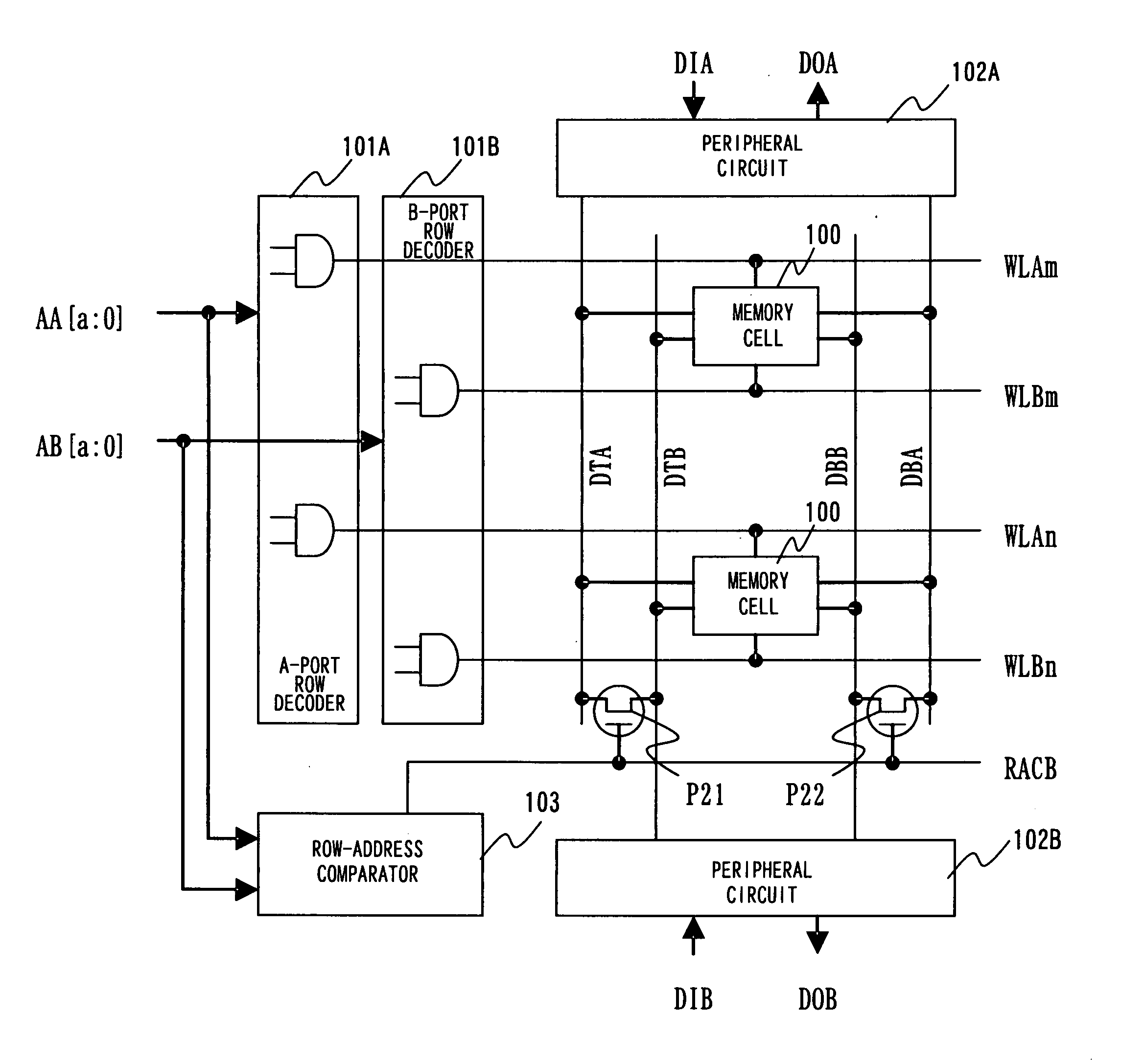
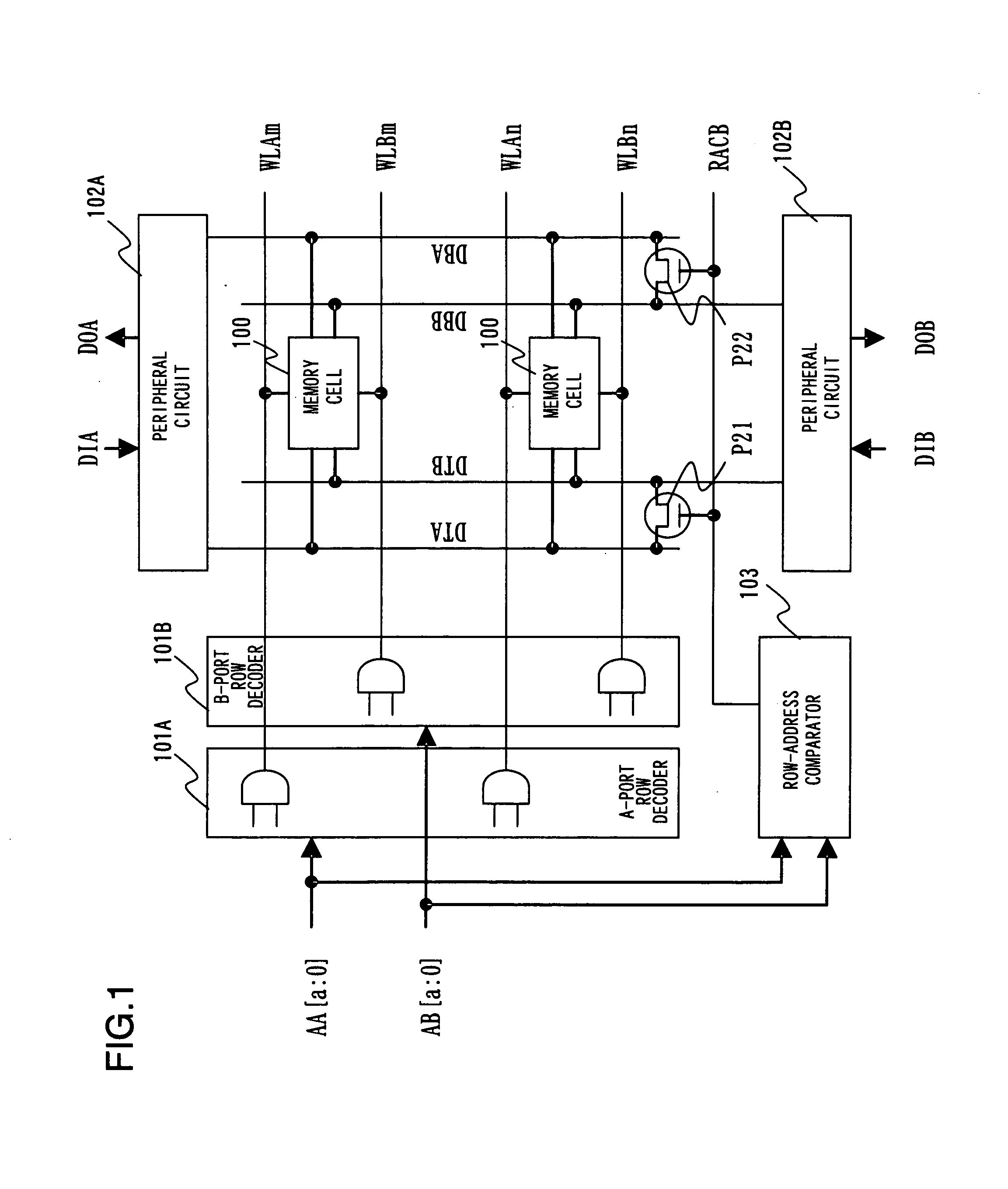
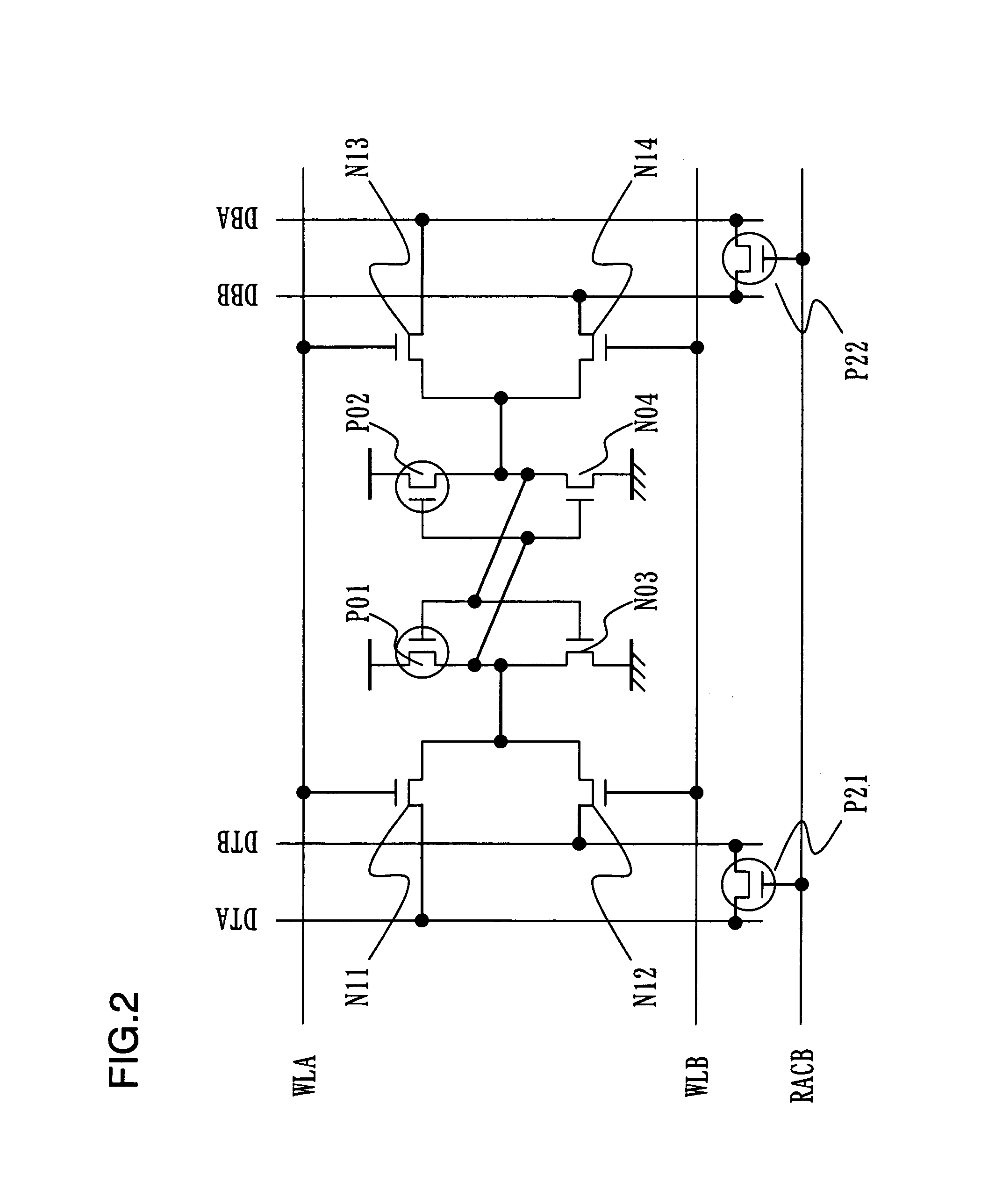
[0078]The present invention will now be described in detail with reference to the accompanying drawings. The present invention is such that even in case where there are variations in ON currents of access transistors in a multiport RAM (inclusive of a dual-port RAM) connected to word lines of a plurality of ports and to bit lines of the plurality of ports, equal currents flow into the bit lines of A and B ports through inter-port switches when at the time of the same-row-address access, thereby eliminating the effects of port-to-port variation in ON currents of the access transistors and preventing malfunction due to erroneous read.

[0079]Even in a case where accessing of A and B ports is asynchronous and random, since the clock is not that of a single channel and operation is possible asynchronously, use in random access is possible. Similarly, the effect of port-to-port variation in ON currents of access transistors is eliminated at this time as well so that malfunction due to erro...


PUM


Abstract

Disclosed is a semiconductor memory device including a plurality of memory cells, each of which is connected to word lines of first and second ports and to bit lines of the first and second ports, and first and second inter-port switches for electrically connecting first bit lines of the first port and second bit lines of the second port when row addresses of the first and second ports match each other.

Description

REFERENCE TO RELATED APPLICATION[0001]This application is based upon and claims the benefit of the priority of Japanese patent application No. 2007-165087, filed on Jun. 22, 2007, the disclosure of which is incorporated herein in its entirety by reference thereto.TECHNICAL FIELD[0002]This invention relates to a semiconductor memory device and, more particularly, to semiconductor memory device having a cell with a plurality of ports.BACKGROUND[0003]With the progress in micro-fabrication technologies of semiconductors, the dimension of transistors has so shrunk that the influence of variations in transistor characteristics becomes more remarkable as compared with a case where the dimension of transistors is large. If a variation in transistor characteristics (a difference in ON current between transistors of the same size having identical capabilities) is too large, this can lead to malfunction, namely an inability to perform memory-cell data read / write, by way of example. If operatin...

Claims


Application Information

Patent Timeline
IPC IPC(8): G11C8/00
CPCG11C8/16G11C11/417
Inventor KINOSHITA, MASAAKIMITOH, HIDEKI
Owner NEC ELECTRONICS CORP
Why Eureka
Try Eureka