Miniature high-voltage power supplies
- Summary
- Abstract
- Description
- Claims
- Application Information
AI Technical Summary
Benefits of technology
Problems solved by technology
Method used
Image
Examples
Embodiment Construction
[0023]The present invention provides power circuitry and power supplies for use in powering high-voltage devices where the available input voltage is relatively low and is required to be “stepped up” to a relatively high voltage to adequately power the device. While the subject invention may be employed with any high-voltage device, the invention is particularly described in the context of a device which provides a capacitive load. Still yet, for purposes of illustration only, the capacitive load used in the context of this description is a dielectric elastomer / electroactive polymer transducer, which is described in greater detail below.
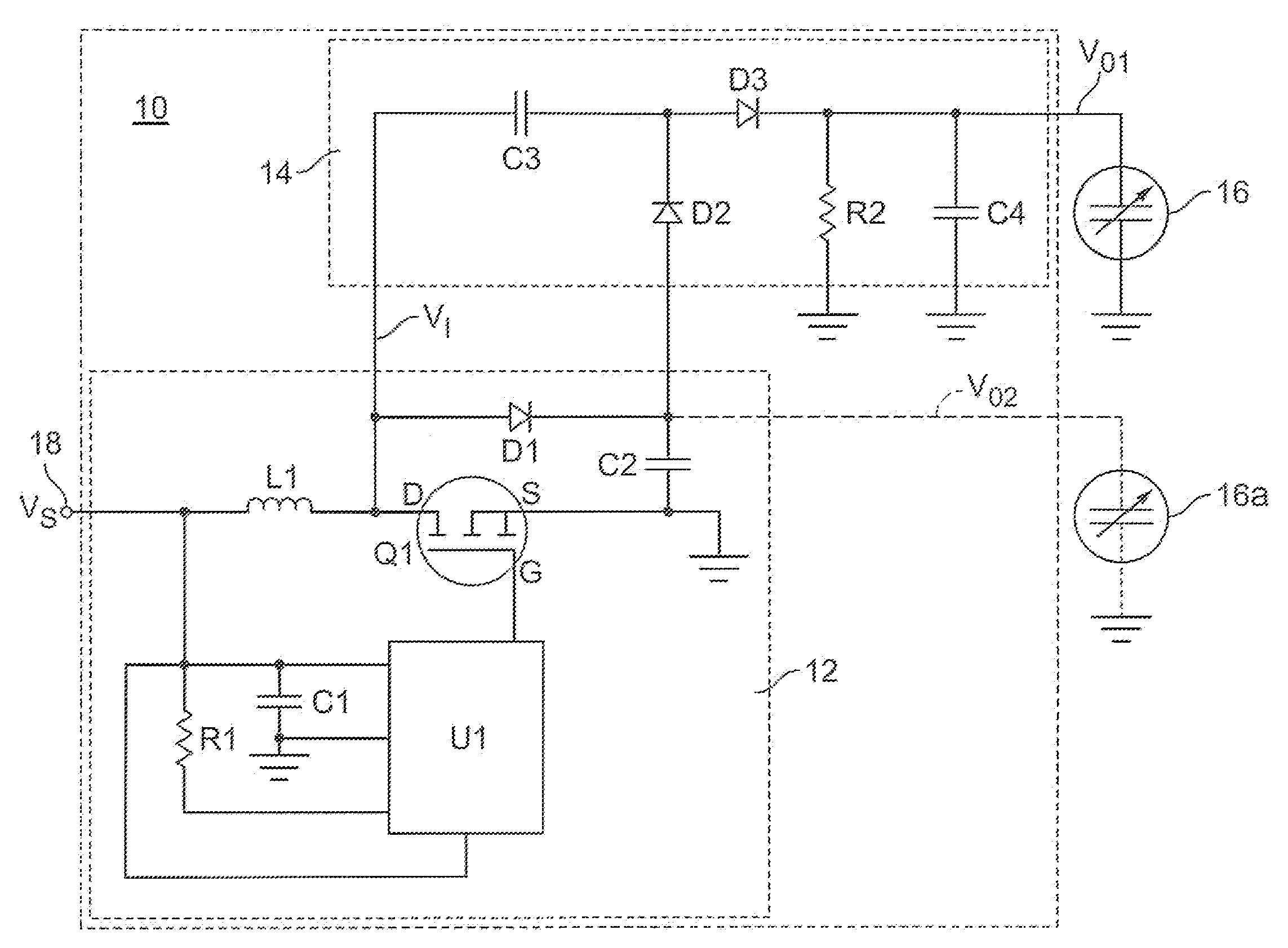
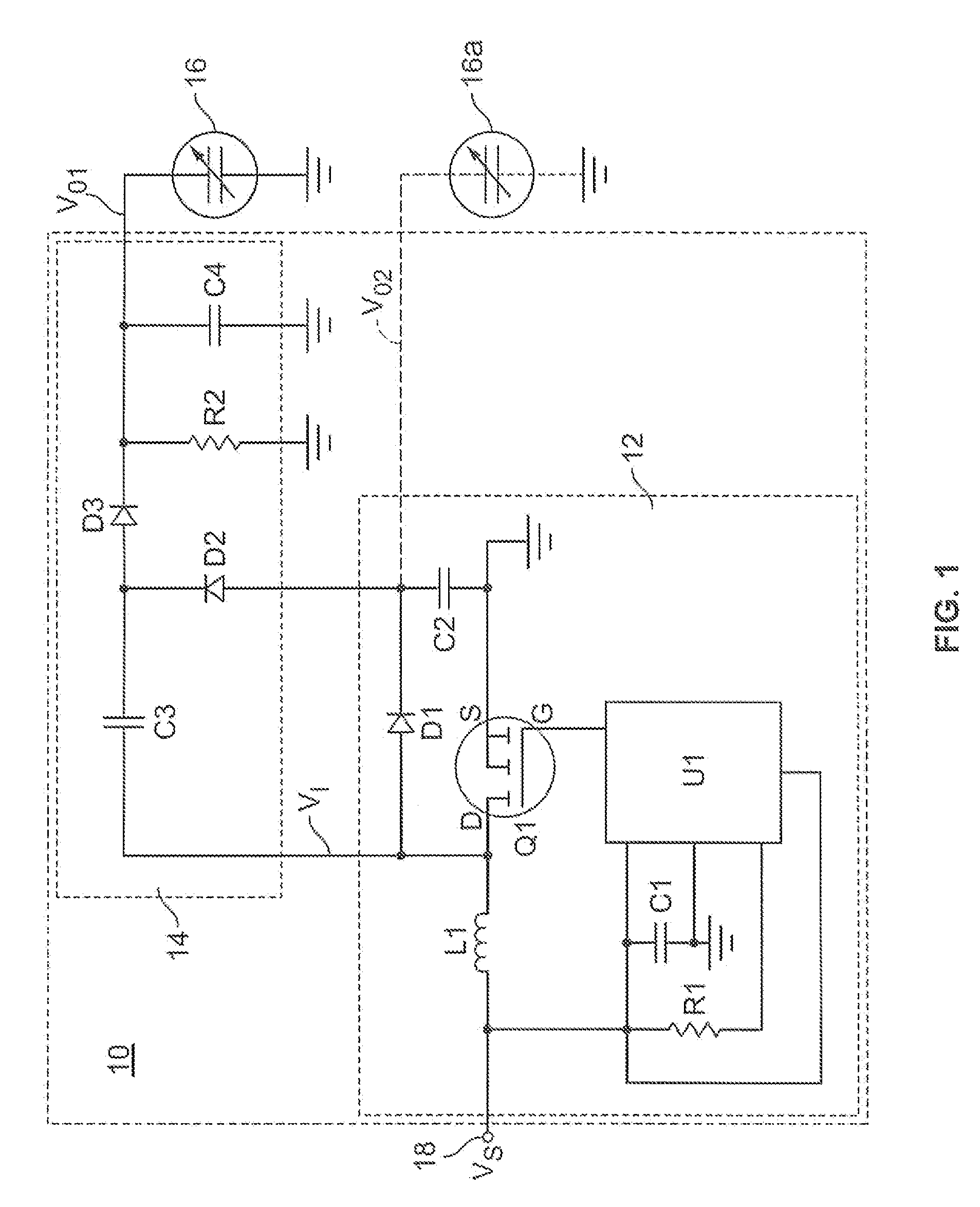
[0024]A general configuration of a power supply 10 of the present invention is provided in the block diagram of FIG. 1. In general, power supply 10 includes power circuit 12 and voltage multiplier circuit 14. Power circuit 12 has an input 18 coupled to a relatively low DC source signal VS (e.g., 2 to 5 volt range) and an output coupled to the input s...
PUM
 Abstract
Description
Claims
Application Information
 - R&D
- Intellectual Property
- Life Sciences
- Materials
- Tech Scout
- Unparalleled Data Quality
- Higher Quality Content
- 60% Fewer Hallucinations
Browse by: Latest US Patents, China's latest patents, Technical Efficacy Thesaurus, Application Domain, Technology Topic, Popular Technical Reports.
© 2025 PatSnap. All rights reserved.Legal|Privacy policy|Modern Slavery Act Transparency Statement|Sitemap|About US| Contact US: help@patsnap.com


