Piezoelectric substance and piezoelectric element
a piezoelectric element and piezoelectric technology, applied in the field of piezoelectric elements and piezoelectric substances, can solve the problems of noticeable property variation and degradation, unnegligible effect, and the inability to produce high-sensitivity sensors
- Summary
- Abstract
- Description
- Claims
- Application Information
AI Technical Summary
Benefits of technology
Problems solved by technology
Method used
Image

Examples
examples
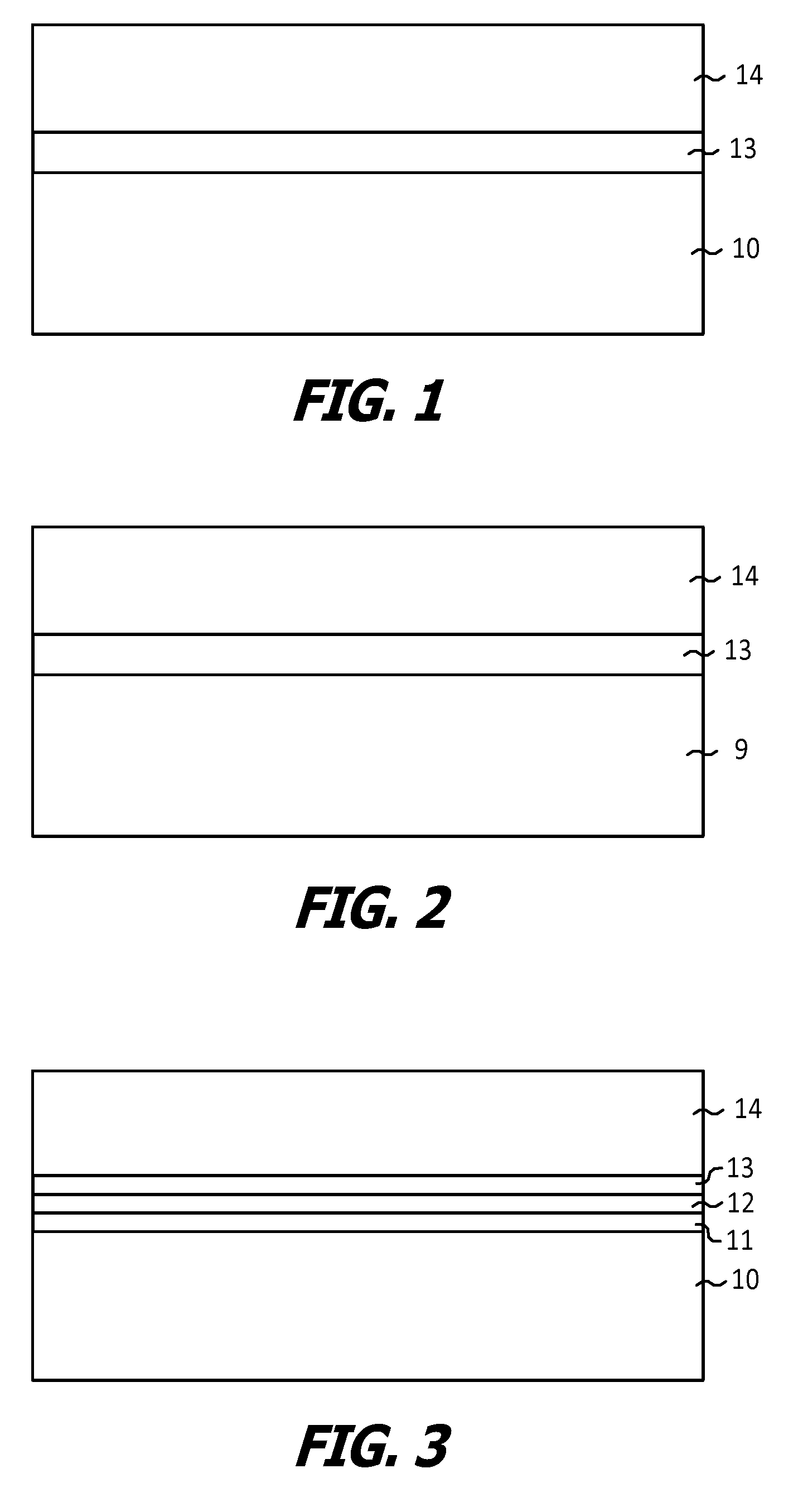
[0060]Examples 1 and 2 and Comparison example will be explained where piezoelectric substance samples are formed that include a 3 μm-thick LKNN film as a piezoelectric film.
example 1
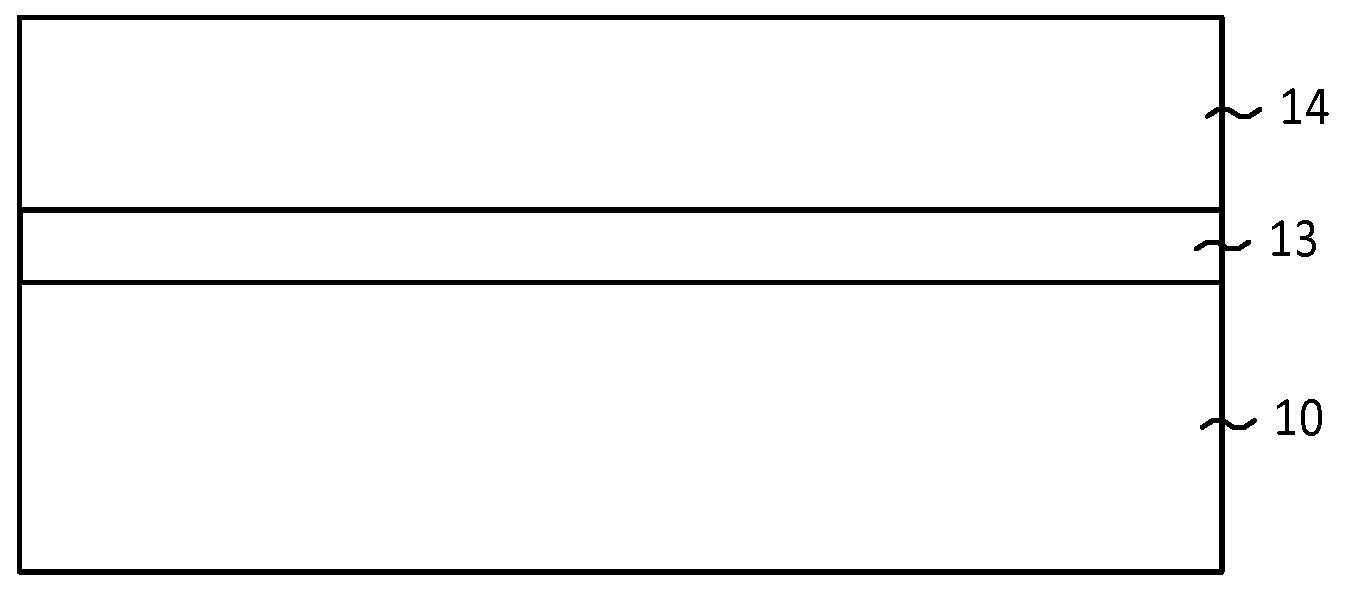
[0061]First, prepared is a substrate with an electrode on which an LKNN film 14 is to be formed.
[0062]As shown in FIG. 1, the substrate uses a Si (001) substrate 10 not oxidized thermally. Formed directly on this thermally oxidized film-free Si substrate 10 is a Pt electrode 13. The film formation of this Pt electrode 13 uses sputtering. The substrate temperature is 300° C., and the film formation is performed at 700° C. so as to inherit the crystallinity of the underlying Si substrate 10 of the Pt electrode 13. When the Pt electrode 13 is formed directly on the Si substrate 10, the Pt crystals are -axis-oriented in the direction normal to the surface of the Si substrate 10, and the axes of the axially oriented Pt crystals are also aligned in the same direction in the in-plane direction of the Si substrate 10. In this manner, the substrate with the electrode is prepared in which the Pt crystals of the electrode are arranged regularly in the in-plane direction as well.
[0063]Next, for...
example 2
[0064]As shown in FIG. 2, in the same conditions as in Example 1, except that the substrate uses a MgO substrate 9, a Pt electrode 13 is formed directly on the MgO substrate 9. When the Pt electrode 13 is formed directly on the MgO substrate 9, as in Example 1, the Pt crystals are -axis-oriented in the direction normal to the surface of the MgO substrate 9, and the axes of the axially oriented Pt crystals are also aligned in the same direction in the in-plane direction of the MgO substrate 9. On this Pt electrode 13 in the same conditions as in Example 1 is formed a 3 μm-thick LKNN film 14, which results in the piezoelectric substance that includes the 3 μm-thick LKNN film 14.
PUM
| Property | Measurement | Unit |
|---|---|---|
| Piezoelectricity | aaaaa | aaaaa |
Abstract
Description
Claims
Application Information
 - R&D
- Intellectual Property
- Life Sciences
- Materials
- Tech Scout
- Unparalleled Data Quality
- Higher Quality Content
- 60% Fewer Hallucinations
Browse by: Latest US Patents, China's latest patents, Technical Efficacy Thesaurus, Application Domain, Technology Topic, Popular Technical Reports.
© 2025 PatSnap. All rights reserved.Legal|Privacy policy|Modern Slavery Act Transparency Statement|Sitemap|About US| Contact US: help@patsnap.com