Silicon carbide semiconductor device having junction barrier schottky diode
- Summary
- Abstract
- Description
- Claims
- Application Information
AI Technical Summary
Benefits of technology
Problems solved by technology
Method used
Image
Examples
first embodiment
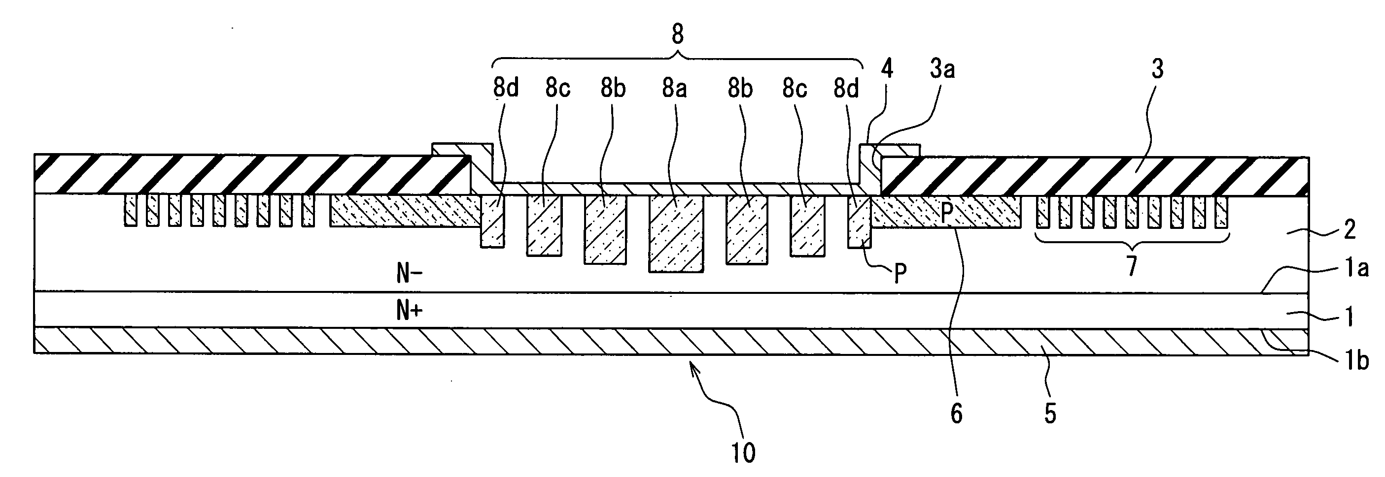
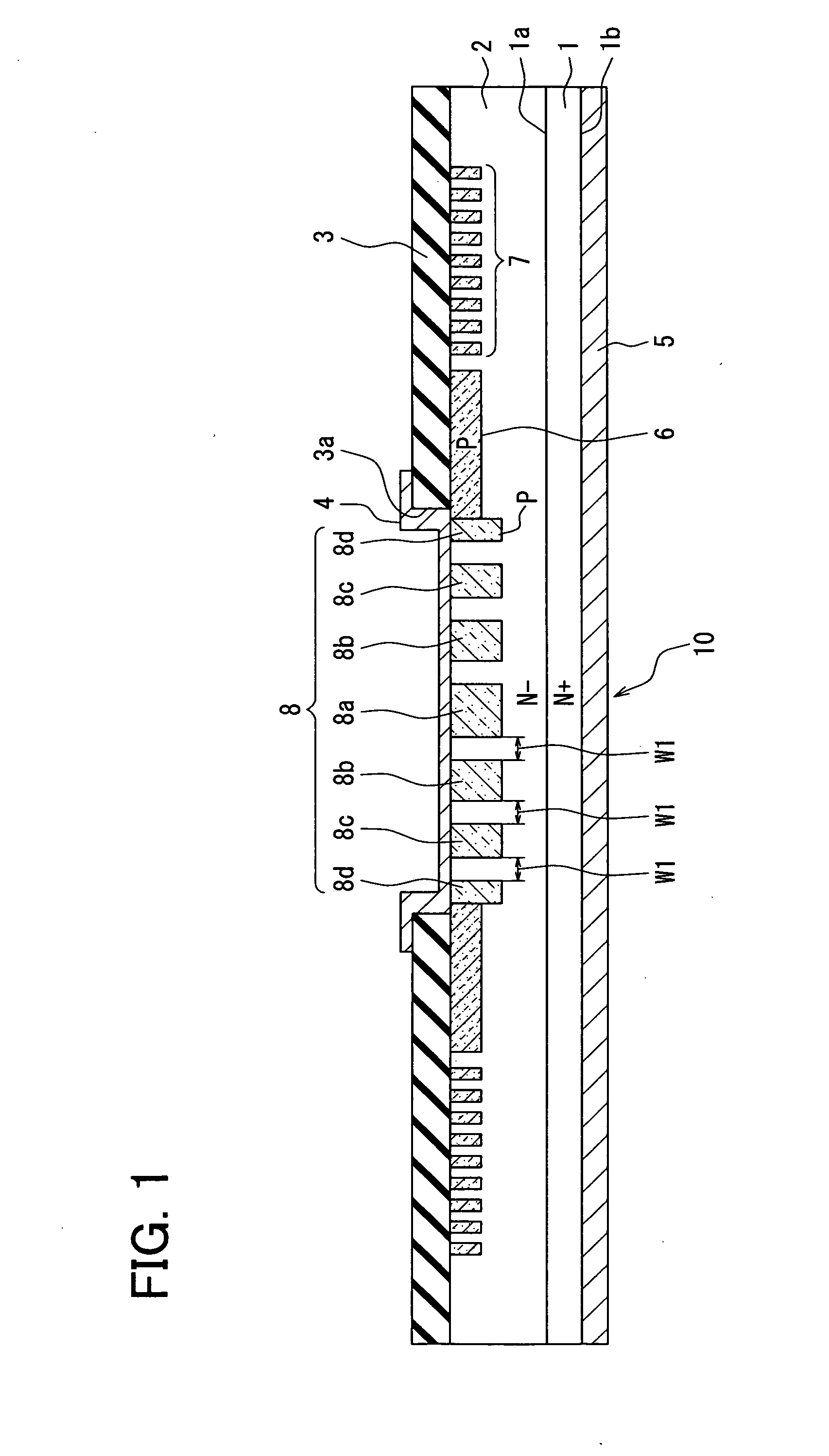
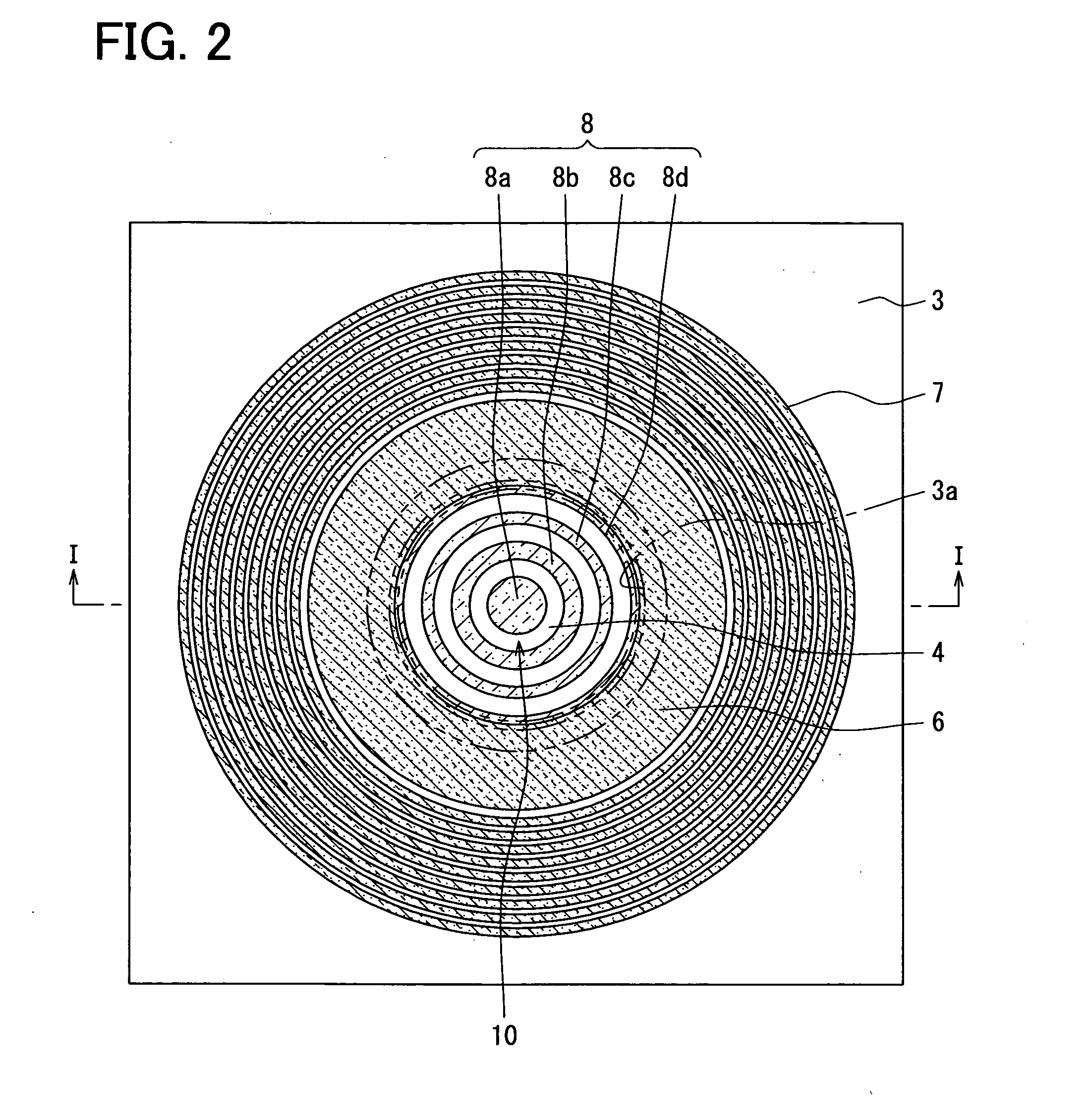
[0020]An SiC semiconductor device having a JBS according to a first embodiment is described below with reference to FIGS. 1 and 2.
[0021]The SiC semiconductor device includes an N+type substrate 1 made of SiC, the N−type drift layer 2 made of SiC. An impurity concentration of the N+type substrate 1 is in a range, for example, between 2×1018 cm−3 and 1×1021 cm−3. The N+type substrate 1 includes a top surface la and a bottom surface 1b opposite to each other. The top surface 1a and the bottom surface 1b are also referred to hereinafter as a principal surface 1a and a rear surface 1b, respectively. The N−type drift layer 2 made of SiC is disposed on the principal surface 1a. The N−type drift layer 2 may be a stacked layer. A dopant concentration of the N−type drift layer 2 is, for example, in a range between 2.5×1015 cm−3 and 7.5×1015 cm−3 and lower than that of the N+type substrate 1. A portion of the N+type substrate 1 and a portion of the N−type drift layer 2 provide a cell where an ...
second embodiment
[0039]An SiC semiconductor device having a JBS according to a second embodiment is described below with reference to FIG. 4. Geometry of P type layers 8 according to the present embodiment is different from that of the P type layers 8 according to the first embodiment.
[0040]As shown in FIG. 4, a depth of each P type layer 8 is deeper than that of the P type resurf layer 6 and the P type guard ring layers 7 in a direction, for example, substantially perpendicular to the principal surface 1a of the substrate 1. The P type resurf layer 6 and the P type guard ring layers 7 are included in the termination structure. The depth of each P type layer 8 is, for example, in a range between 0.7 μm and 1.5 μm. A depth difference between each P type layer 8 and the P type resurf layer 6 is in a range between 0.2 μm and 1.0 μm. A depth difference between each P type layer 8 and each P guard ring layer 7 is also in the range between 0.2 μm and 1.0 μm.
[0041]Since each P type layer 8 is deeper than t...
third embodiment
[0042]An SiC semiconductor device having a JBS according to a third embodiment is described below with reference to FIG. 6. Depths of P type layers 8 according to the present embodiment are different from that of the P type layers 8.according to the first and second embodiments.
[0043]As shown in FIG. 6, a depth of one of the multiple P type layers is less than or equal to that of another one of the multiple P type layers, wherein the another one is disposed adjacent to the one of the multiple P type layers 8 and disposed closer to the center of the contact region than the one of the multiple P type layers 8. Some of the P type layers located around the center member 8a are configured to have a substantially equal depth. According to the above structure, when a depletion layer is created below a central portion of the contact region between the Schottky electrode 4 and the N−type drift layer 2, the depletion layer is located in a deep portion of the N−type drift layer 2. An electric ...
PUM
 Abstract
Description
Claims
Application Information
 - R&D
- Intellectual Property
- Life Sciences
- Materials
- Tech Scout
- Unparalleled Data Quality
- Higher Quality Content
- 60% Fewer Hallucinations
Browse by: Latest US Patents, China's latest patents, Technical Efficacy Thesaurus, Application Domain, Technology Topic, Popular Technical Reports.
© 2025 PatSnap. All rights reserved.Legal|Privacy policy|Modern Slavery Act Transparency Statement|Sitemap|About US| Contact US: help@patsnap.com


