Method for adhering semiconductor devices

a technology of semiconductor devices and semiconductor components, applied in semiconductor devices, semiconductor/solid-state device details, electrical apparatus, etc., can solve the problems of deteriorating electrical and physical properties of semiconductor devices, cracking of deep via conductors, and difficult realization of various devices having different design rules on one chip, so as to prevent cracking of semiconductor devices, wide area, and dissipate thermal energy generated by semiconductor devices

Inactive Publication Date: 2008-11-20
DSS TECH MANAGEMENT
View PDF2 Cites 6 Cited by
  • Summary
  • Abstract
  • Description
  • Claims
  • Application Information

AI Technical Summary

Benefits of technology

[0006]Embodiments consistent with the present invention provide a method for adhering semiconductor devices including forming a heat sink via having a wide area. When semiconductor devices are adhered to each other, the heat sink via may dissipate thermal energy generated by the semiconductor devices, so as to prevent cracking of the semiconductor devices.

Problems solved by technology

However, realizing various devices having different design rules on one chip is very difficult and has many limitations.
Heat generated by a multi-level chip accumulates in the semiconductor devices, and can easily deteriorate the electrical and physical properties of the semiconductor devices.
In a package level, deep via conductors may crack due to the excessive heat accumulated in the semiconductor devices.

Method used


Image

  • Method for adhering semiconductor devices
  • Method for adhering semiconductor devices
  • Method for adhering semiconductor devices

Examples


Embodiment Construction

[0010]Hereinafter, embodiments consistent with the present invention will be described in detail with reference to the accompanying drawings so that they can be readily implemented by those skilled in the art.

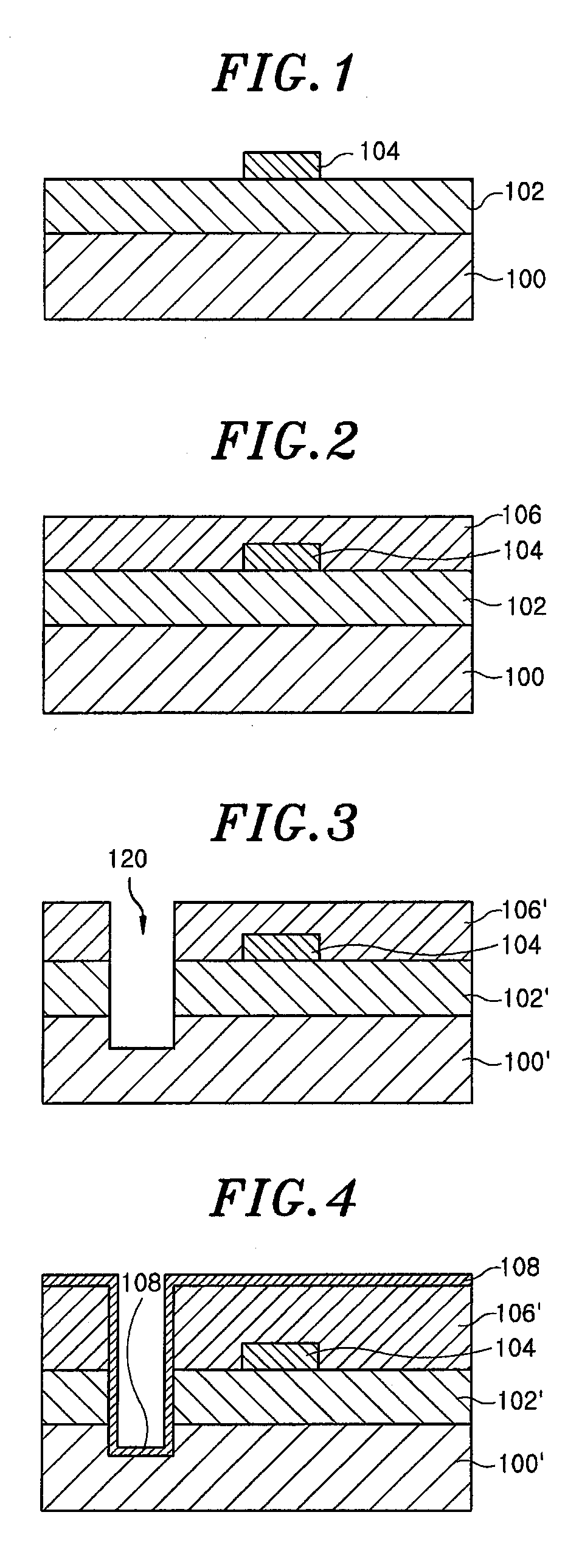
[0011]FIGS. 1 to 17 are sectional views illustrating a method for adhering semiconductor devices in accordance with one embodiment consistent with the present invention.

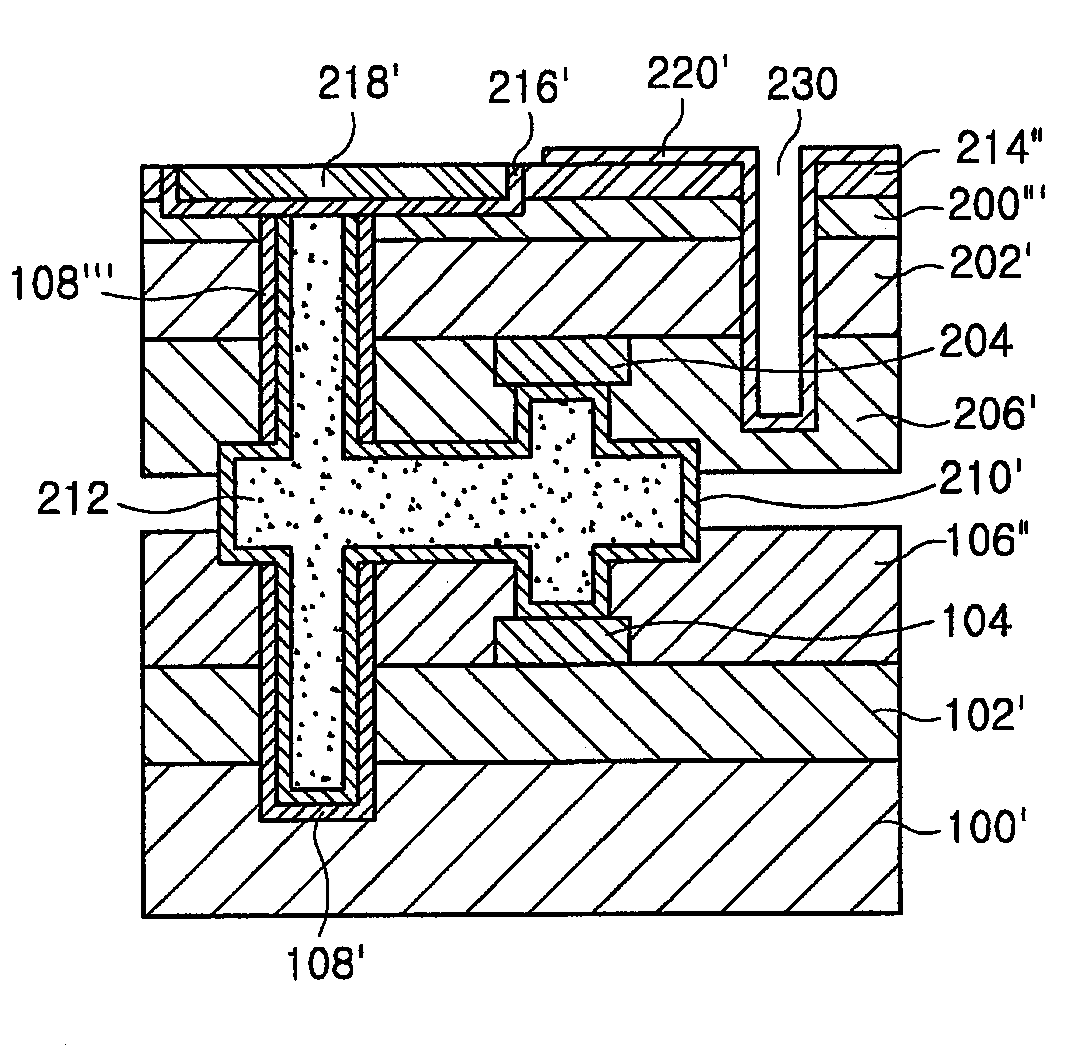
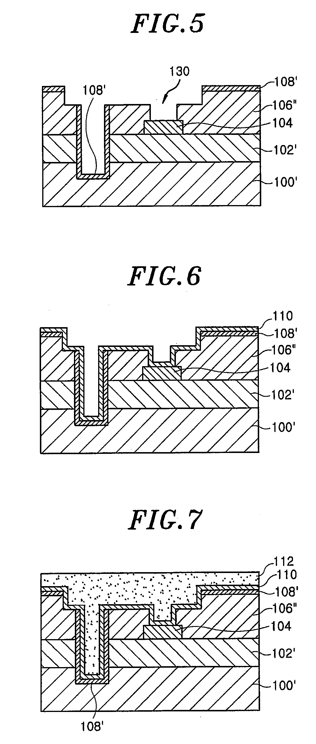
[0012]Specifically, FIGS. 1 to 9 illustrate a process for manufacturing a first semiconductor device consistent with the present invention and FIGS. 10 to 17 illustrate a process for forming a heat sink when a second semiconductor device consistent with the present invention is adhered to the first semiconductor device. As illustrated in FIGS. 1 and 2, after depositing an insulating layer 102 on a semiconductor substrate 100, an upper metal layer 104 is formed on insulating layer 102 and a gap fill layer 106 is formed on upper metal layer 104 and insulating layer 102. In one embodiment, insulating layer 102 may ...


PUM


Abstract

A method for adhering semiconductor devices is provided. The method includes forming a first semiconductor device including a first metal pad, forming a second semiconductor device including a second metal pad, adhering the first semiconductor device to the second semiconductor device, the first metal pad electrically connecting the second metal pad, and forming a heat sink via in the second semiconductor device.

Description

TECHNICAL FIELD[0001]Embodiments consistent with the present invention relate to a method for adhering semiconductor devices, and more particularly, to a method for adhering semiconductor devices capable of preventing a crack phenomenon.RELATED ART[0002]In the semiconductor industry, for example, in system on chip (SOC) technology, researchers have attempted to integrate analog, RF, CPU, and CMOS sensors on one chip. However, realizing various devices having different design rules on one chip is very difficult and has many limitations.[0003]In order to solve such a problem, a system in package (SIP) technology has been introduced. In SIP, two different semiconductor devices are connected to each other by a deep via conductor to reduce chip size and to secure enough storage capacity.[0004]Generally, semiconductor devices are connected through deep via conductors having a high aspect ratio. Heat generated by a multi-level chip accumulates in the semiconductor devices, and can easily d...

Claims


Application Information

Patent Timeline
Patent Type & Authority Applications(United States)
IPC IPC(8): H01L21/58
CPCH01L21/76898H01L23/3677H01L2924/0002H01L2224/05554H01L2924/00014H01L23/481H01L23/585H01L24/03H01L24/05H01L25/0657H01L25/18H01L25/50H01L2224/0557H01L2224/05599H01L2225/06541H01L2225/06589H01L2924/01013H01L2924/01022H01L2924/01029H01L2924/01047H01L2924/01073H01L2924/01074H01L2924/01079H01L2924/014H01L2924/30105H01L2924/01006H01L2924/01033H01L2224/05552H01L21/28
Inventor JUNG, OH JIN
Owner DSS TECH MANAGEMENT
Why Eureka
Try Eureka