
Liquid crystal display device and image display method thereof

Active Publication Date: 2008-11-13
JVC KENWOOD CORP A CORP OF JAPAN
View PDF14 Cites 77 Cited by
  • Summary
  • Abstract
  • Description
  • Claims
  • Application Information

AI Technical Summary

Benefits of technology

[0014]According to this embodiment of a liquid crystal display device, the backlight device is divided into multiple regions and the emission luminance of a backlight for each region is controlled by the strength of an image signal. With this control, variations in brightness and color among the regions can be reduced. Accordingly, the quality of an image displayed on the liquid crystal panel can be improved. Moreover, when the emission luminance is made non-uniform, the power consumption of the backlight device can be further reduced.

Problems solved by technology

A large share of power consumption by a conventional liquid crystal display device is for the backlight device.
Therefore, a liquid crystal display device has a problem of needing a large power consumption in order to keep the backlight in the constant lighting state.
As a result, this produces the problem that an image displayed on the liquid crystal panel differs from an original image.
For this reason, the foregoing problem is particularly acute due to change in temperatures of the LED devices and due to age deterioration of the LED devices.
In the configuration wherein the regions are completely separated from each other, it is difficult to determine the locations of adjacent regions of a particular pixel located above a boundary between the adjacent regions.
For this reason, the configuration described in Non-patent Document 1 is not very useful.

Method used


Image

  • Liquid crystal display device and image display method thereof
  • Liquid crystal display device and image display method thereof
  • Liquid crystal display device and image display method thereof

Examples


first embodiment

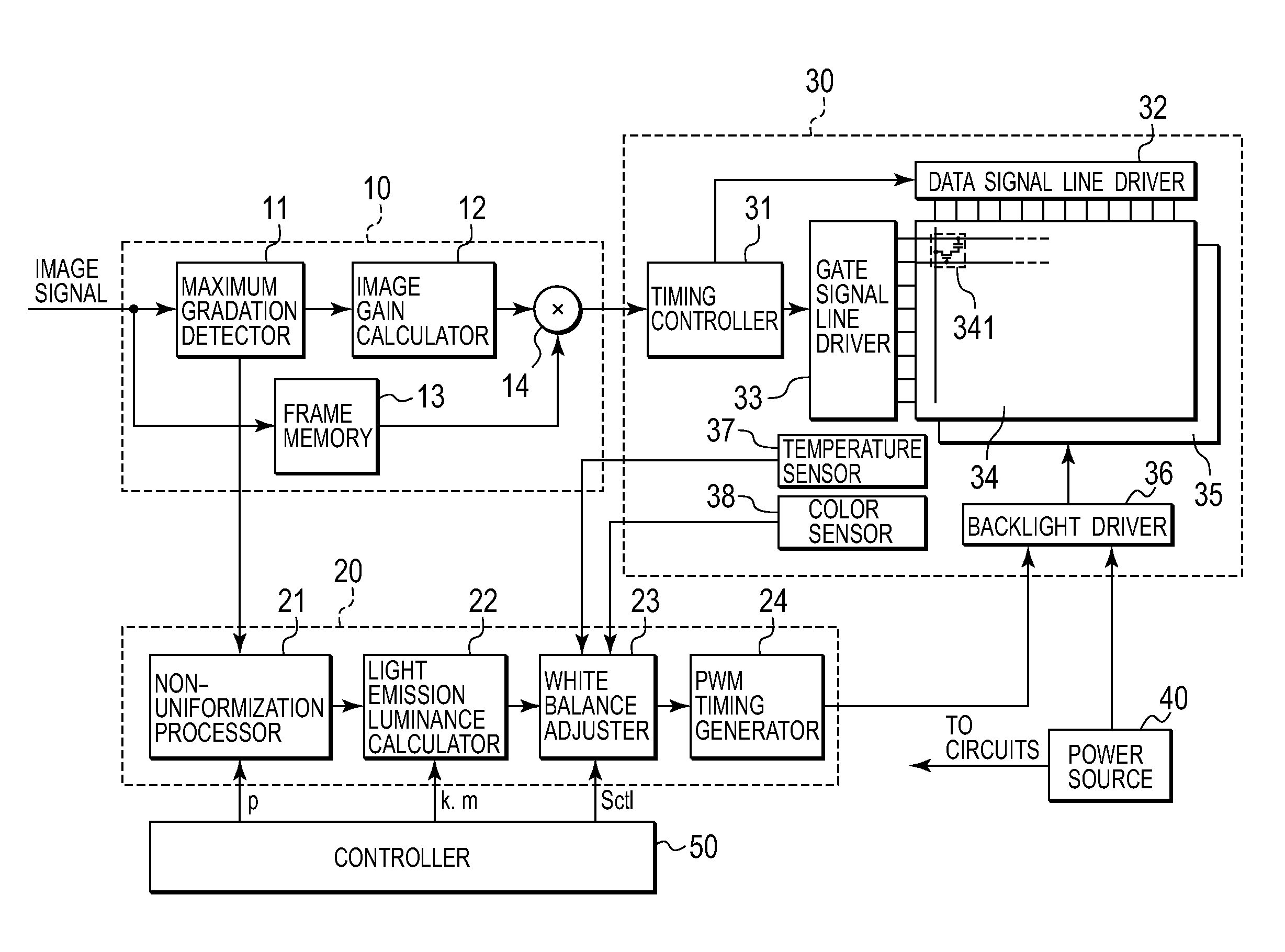
[0049]A liquid crystal display device of a first embodiment and an image display method to be used in this device will be described below with reference to the accompanying drawings. FIG. 1 is a block diagram showing an entire configuration of the liquid crystal display device of the first embodiment. In FIG. 1, an image signal to be displayed on liquid crystal panel 34 in liquid module unit 30, which will be described later, is supplied to a maximum gradation detector 11 and frame memory 13 in image signal processor 10. As will be described later in detail, backlight device 35 is divided into a plurality of regions, and liquid crystal panel 34 is divided into a plurality of regions so that these divided regions, respectively, correspond to the divided regions of backlight device 35, whereby luminance of the backlight (amount of light) is controlled in every region of liquid crystal panel 34.

[0050]FIG. 2 is a view showing an example of region divisions of liquid crystal panel 34 and...

second embodiment

[0105]FIG. 21 is a block diagram showing the entire configuration of a liquid crystal display device of a second embodiment. In FIG. 21, the parts that are the same as those shown in FIG. 1 are given the same reference numerals, so that further description thereof is omitted. Further, for the sake of simplicity in, the configuration of FIG. 21, the non-uniformization processor 21 of FIG. 1 has been eliminated, but this may include non-uniformization processor 21 in FIG. 1 as in the first embodiment.

[0106]As described above, in the first embodiment, light emission luminance calculator 22 calculates light emission luminances Bo of lights from light sources 352 themselves of multiple regions of backlight device 35, and causes each light source 352 of multiple regions to emit light. The light emission luminances Bo each indicate a luminance value at the center of each one of the regions. FIG. 22A shows luminance distribution in the case where only region 35b emits light. Here, region 35...

third embodiment

[0112]FIG. 26 is a block diagram showing an entire configuration of a liquid crystal display device of a third embodiment. In FIG. 26, the parts which are the same as those shown in FIG. 1, are given the same reference numerals, so that a further description thereof is omitted. Further, for the sake of simplicity, the non-uniformization processor 21 in FIG. 1 has been eliminated from FIG. 26, but may include as in the case of the first embodiment. Further, the amount-of-emitted light calculator unit 25 has been included in FIG. 26 as in the second embodiment, but also may be eliminated.

[0113]FIG. 27A is a view showing the case where liquid crystal panel 34A is divided into regions 34a to 34d so that regions 34a to 34d correspond to regions 35a to 35d of backlight device 35A respectively. This figure also shows the case where the gradations of regions 34a, 34b, and 34d are zero (i.e., black), and the gradation of region 34c is at maximum gradation 255 (i.e., white). In this case, lig...


PUM


Abstract

A backlight device is divided into multiple regions, and has a configuration in which light emitted from a light source of each of the regions is allowed to leak to other regions. A maximum gradation detector detects a maximum gradation of a regional image signal displayed on each of the regions of the liquid crystal panel. An image gain calculator obtains a gain to be multiplied to each regional image signal. An emission luminance calculator obtains an emission luminance of light to be emitted by each light source, by using an operation expression according to the emission luminance of light to be emitted by the backlight device. At this time, if the emission luminance takes a negative value as a result of calculation, the emission luminance calculator makes a correction so that the emission luminance can take a value equal to or greater than 0.

Description

CROSS REFERENCE TO RELATED APPLICATIONS[0001]This application claims priority based on 35 USC 119 from prior Japanese Patent Applications No. P2007-123136 filed on May 8, 2007, No. P2007-209818 filed on Aug. 10, 2007, No. P2007-209819 filed on Aug. 10, 2007, and No. P2007-209820 filed on Aug. 10, 2007, the entire contents of which are incorporated herein by reference.BACKGROUND OF THE INVENTION[0002]1. Field of the Invention[0003]The present invention relates to a liquid crystal display device having a backlight device, and to an image display method for displaying an image signal while controlling light emission of the backlight device.[0004]2. Description of the Related Art[0005]In a liquid crystal display device displaying an image using a liquid crystal panel, the liquid crystal panel itself does not emit light. Therefore, a backlight device is provided, for example, on the back of the liquid crystal panel. The liquid crystal in the panel is switched between an OFF state and an ...

Claims


Application Information

Patent Timeline
IPC IPC(8): G02F1/13357G09G3/36
CPCG09G3/342G09G3/3426G09G3/3611G09G3/3648G09G2320/0233G09G2320/0271G09G2320/0285G09G2320/041G09G2320/0646G09G2320/0666G09G2330/021G09G2360/145G09G2360/16G02F1/133
Inventor OHSHIMA, YOSHINORI
Owner JVC KENWOOD CORP A CORP OF JAPAN
Learn More