High voltage current splitter circuit and method
a splitter circuit and high voltage technology, applied in the direction of resistive welding apparatus, welding electric supply, electric variable regulation, etc., can solve the problem that the conventional current mirror cannot offer this level of circuit protection, and achieve the effect of higher or lower impedan
- Summary
- Abstract
- Description
- Claims
- Application Information
AI Technical Summary
Benefits of technology
Problems solved by technology
Method used
Image
Examples
first embodiment
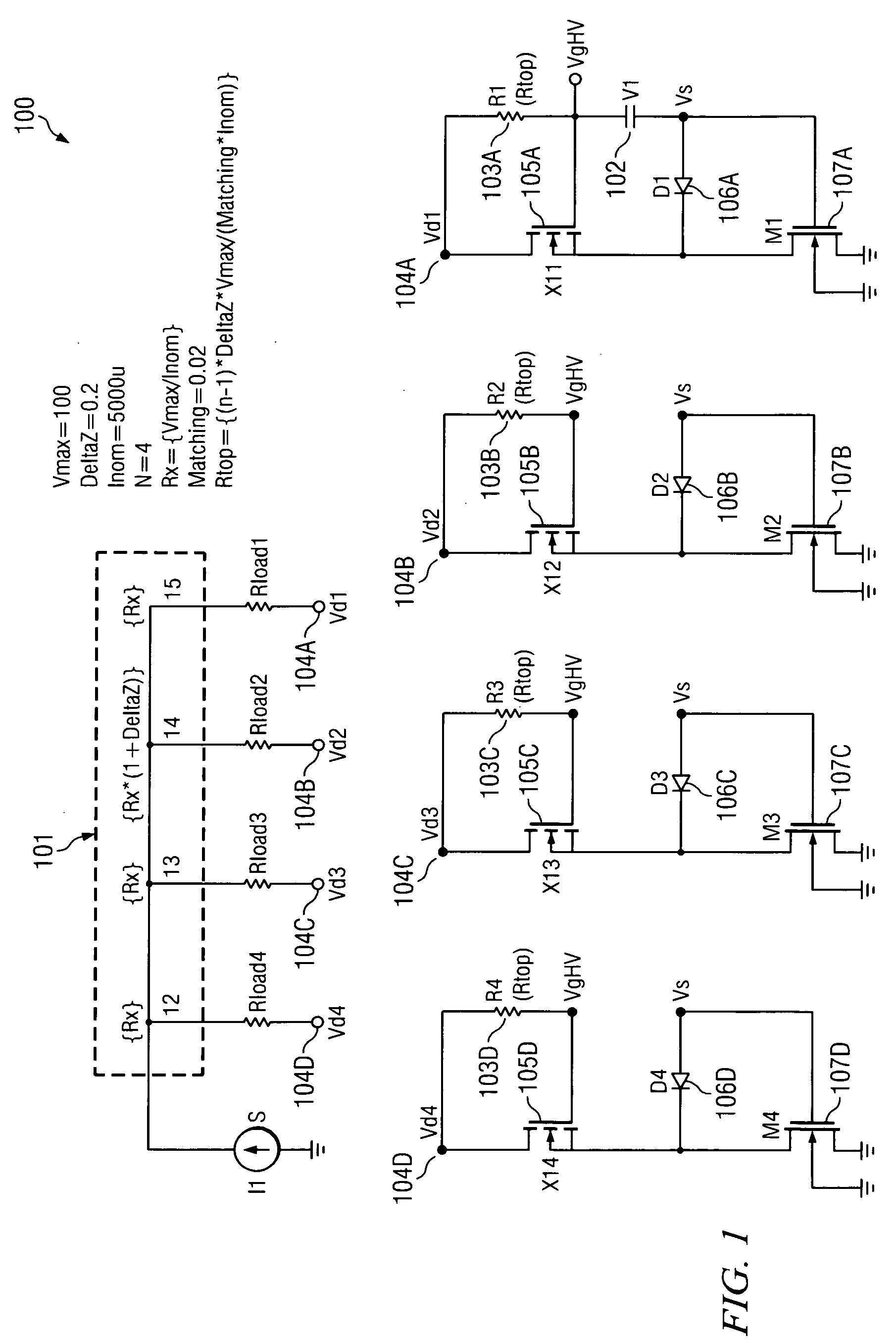
[0016]Referring now to FIG. 1, the present invention is shown in which current is divided in four (4) branches (I2, I3, I4, I5) (each branch also referred to as a sub-circuit), although the present invention can be extended to any N of branch circuits. As seen therein, element V1 102 is biased by a small current flowing through resistors R1, R2, . . . RN, 103A, 103B, 103C and 103D. Element V1 can comprise a bipolar transistor or a MOSFET connected as a diode (gate to drain or base to collector). Element V1 can be any non-linear impedance device having I-V characteristics somewhat similar to a diode.
[0017]The node input Vd1, Vd2 . . . VdN, 104A, 104B, 104C, and 104D, which has the lowest voltage, pulls down the source of its respective transistor X11, X12, or X1N, 105A, 105B, 105C or 105D and forward biases respective diode D1, D2 or DN, 106A, 106B, 106C or 106D. The voltage across element V1 is chosen such that at some current and bias typical of the load operation conditions, the v...
second embodiment
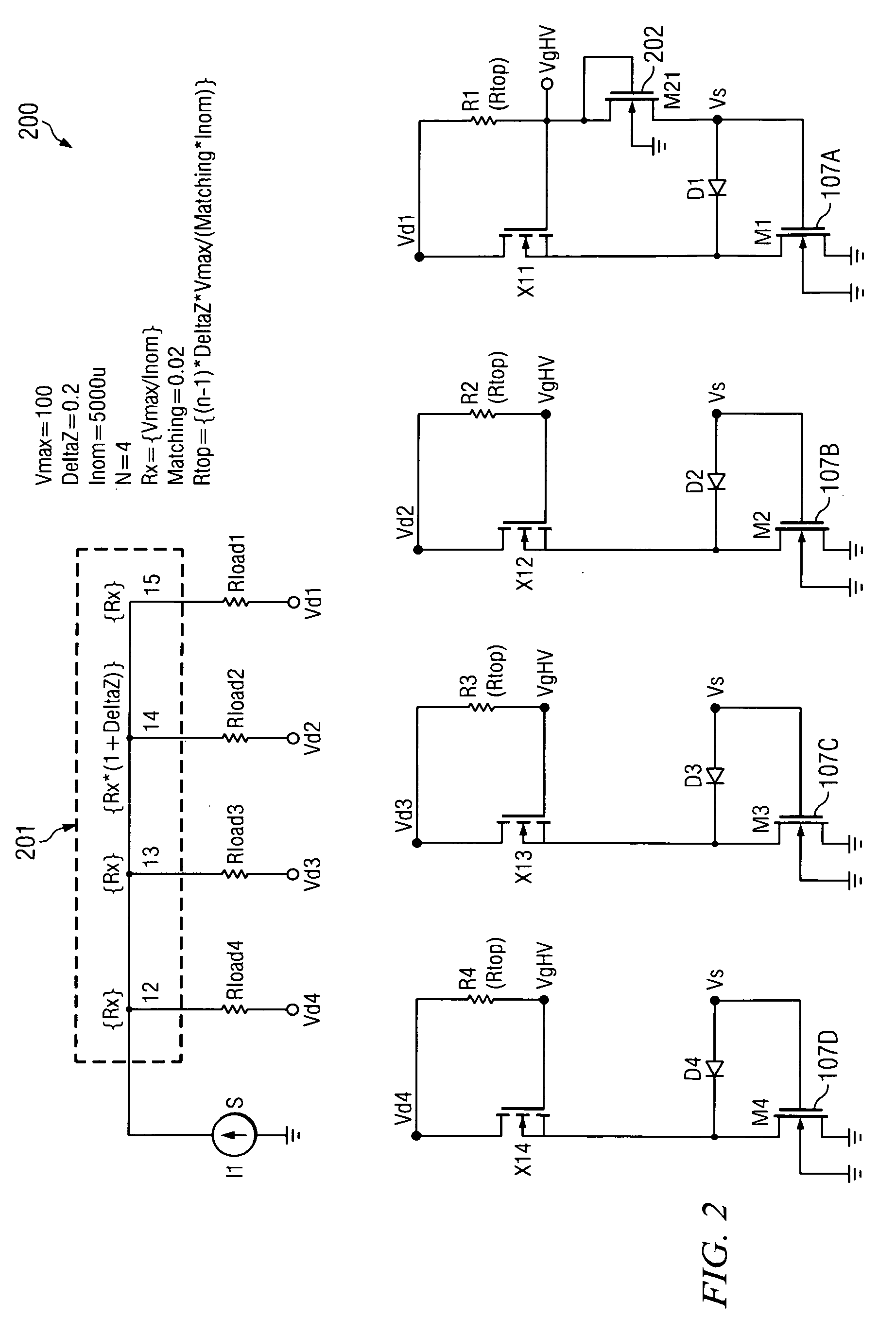
[0019]FIG. 2 provides the circuit 200 of the present invention. The circuit of FIG. 2 is similar to that seen in FIG. 1, provided that element V1102 is replaced by transistor 202 coupled to nodes Vs, VgHV and ground as seen therein. As seen therein, voltage VgHV is selected to be somewhat higher than the minimum gate-source voltage of X11, X12, . . . X1N 105A, 105B, 105C, 105D to ensure proper operation in saturation. The advantage of this arrangement is that element 202 has a similar temperature coefficient that M1 and X11 thus rendering design of a wide operating temperature circuit easier.
third embodiment
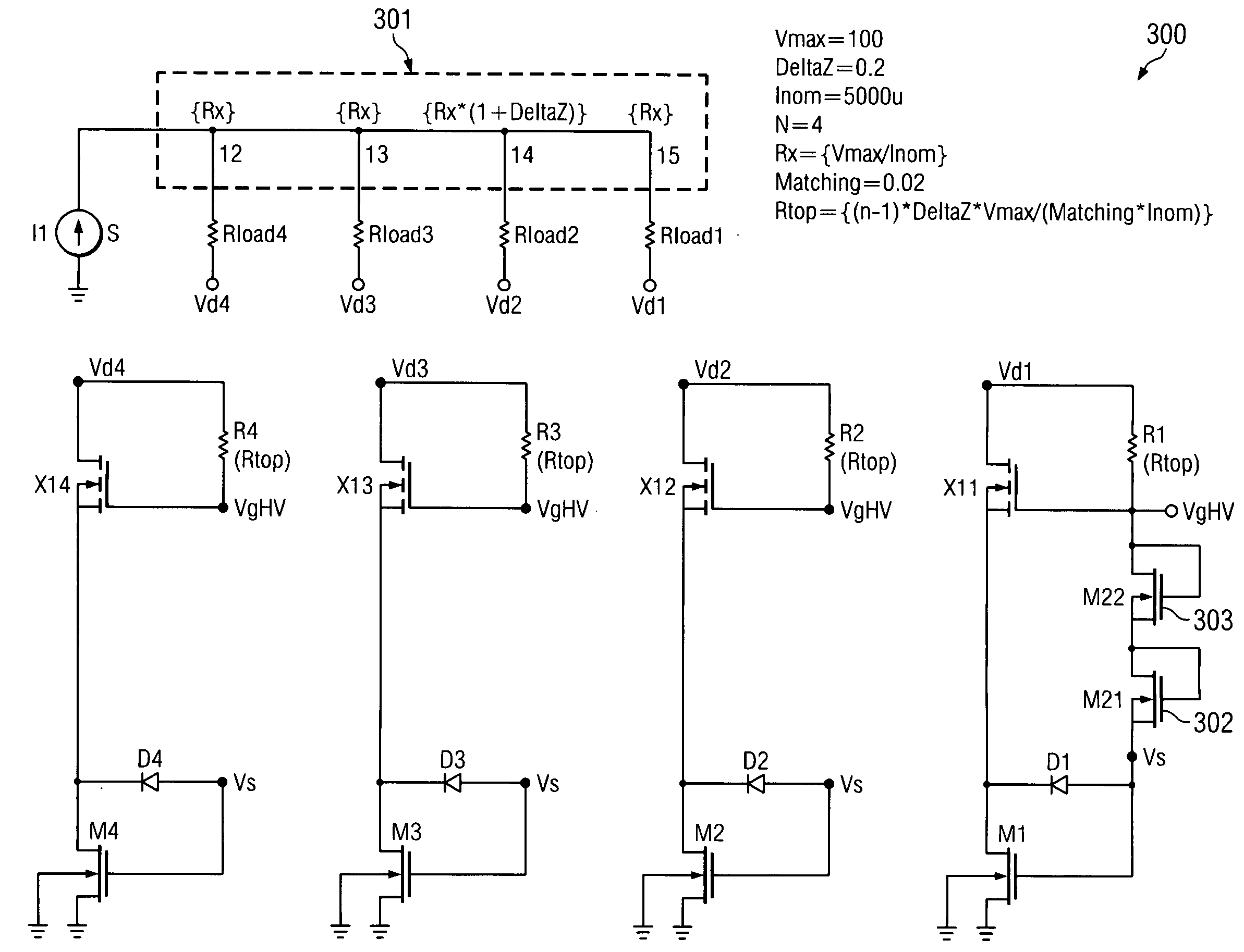
[0020]FIG. 3 provides the circuit 300 of the present invention. The circuit of FIG. 3 is similar to that seen in FIG. 1, provided that element V1102 is replaced by cascoded transistors 302 and 303. The advantage of this arrangement is the cascode transistors each have smaller voltages across them which reduce the chances of transistor damage during transient thus rendering this design more robust in application where transients are a major concern.
PUM
| Property | Measurement | Unit |
|---|---|---|
| voltages | aaaaa | aaaaa |
| voltages | aaaaa | aaaaa |
| frequency | aaaaa | aaaaa |
Abstract
Description
Claims
Application Information
 - R&D
- Intellectual Property
- Life Sciences
- Materials
- Tech Scout
- Unparalleled Data Quality
- Higher Quality Content
- 60% Fewer Hallucinations
Browse by: Latest US Patents, China's latest patents, Technical Efficacy Thesaurus, Application Domain, Technology Topic, Popular Technical Reports.
© 2025 PatSnap. All rights reserved.Legal|Privacy policy|Modern Slavery Act Transparency Statement|Sitemap|About US| Contact US: help@patsnap.com


