Photosensitive composition and pattern forming method using the same

Active Publication Date: 2008-11-06
FUJIFILM CORP
View PDF3 Cites 4 Cited by
  • Summary
  • Abstract
  • Description
  • Claims
  • Application Information

AI Technical Summary

Benefits of technology

[0010]An object of the present invention is to provide a photosensitive composition ensuring that even in the formation of a fine pattern of approximately from several tens to several hundreds nm, the development defect is reduced and the focus margin is wide (that is, the variation in the line width due to fluctuation of the focal position is small), and a pattern forming method using the photosensitive composition.
[0011]As a result of various studies, the present inventors have found that when a compound represented by formula (I-a) and a compound represented by formula (I-b) are used in combination as basic compounds and a compound represented by formula (II) is used as a surfactant, the film loss of the resist is suppressed and this enables enlargement of the focus margin and reduction in the development defect.
[0038]The photosensitive composition of the present invention ensures reduced development defect and wide focus margin even in the formation of a fine pattern of approximately from several tens to several hundreds nm, so that a good fine pattern can be produced with high productivity.

Problems solved by technology

However, in view of integrated performance as the resist, an appropriate combination of the resin, photo-acid generator, basic compound, surfactant, solvent and the like used is actually very difficult to find out, and moreover, it is strongly demanded to satisfy both the resolution performance and the development defect performance.
The development defect may adversely affect the formation and the like of a fine semiconductor device.

Method used


Image

  • Photosensitive composition and pattern forming method using the same
  • Photosensitive composition and pattern forming method using the same
  • Photosensitive composition and pattern forming method using the same

Examples


examples

[0415]The present invention is described in greater detail below by referring to Examples, but the present invention should not be construed as being limited to the following Examples.

[0416]The structures and molecular weights of the resin (C) are shown below.

 (1)Mw = 9700Mw / Mn = 1.81 (2)Mw = 9400Mw / Mn = 1.78 (3)Mw = 13700Mw / Mn = 1.89 (4)Mw = 10300Mw / Mn = 1.90 (5)Mw = 8900Mw / Mn = 1.80 (6)Mw = 7900Mw / Mn = 1.73 (7)Mw = 8300Mw / Mn = 1.81 (8)Mw = 15600Mw / Mn = 2.03 (9)Mw = 9800Mw / Mn = 1.86(10)Mw = 18300Mw / Mn = 2.10(11)Mw = 6900Mw / Mn = 1.71(12)Mw = 8300Mw / Mn = 1.81(13)Mw = 9600Mw / Mn = 1.81(14)Mw = 5800Mw / Mn = 1.69(15)Mw = 4700Mw / Mn = 1.70(16)Mw = 8900Mw / Mn = 1.81(17)Mw = 13900Mw / Mn = 1.98(18)Mw = 12700Mw / Mn = 1.99(19)Mw = 9300Mw / Mn = 1.81(20)Mw = 7600Mw / Mn = 1.76(21)Mw = 12700Mw / Mn = 1.86(22)Mw = 8200Mw / Mn = 1.68(23)Mw = 8500Mw / Mn = 1.77(24)Mw = 8200Mw / Mn = 1.75(25)Mw = 9200Mw / Mn = 1.92(26)Mw = 8200Mw / Mn = 1.65

[0417]The structures of Fluorine Group-Containing Resins (FII-1) to (FII-10) use...

examples ar-1

to AR-30 and Comparative Examples ar1 to ar5

Preparation of Resist

[0419]The components shown in Table 2 below were dissolved in a solvent to prepare a solution having a solid content concentration of 6 mass %, and the obtained solution was filtered through a 0.1-μm polytetrafluoroethylene filter or polyethylene filter to prepare a positive resist solution. The positive resist solutions prepared were evaluated by the following methods, and the results are shown in Table 2.

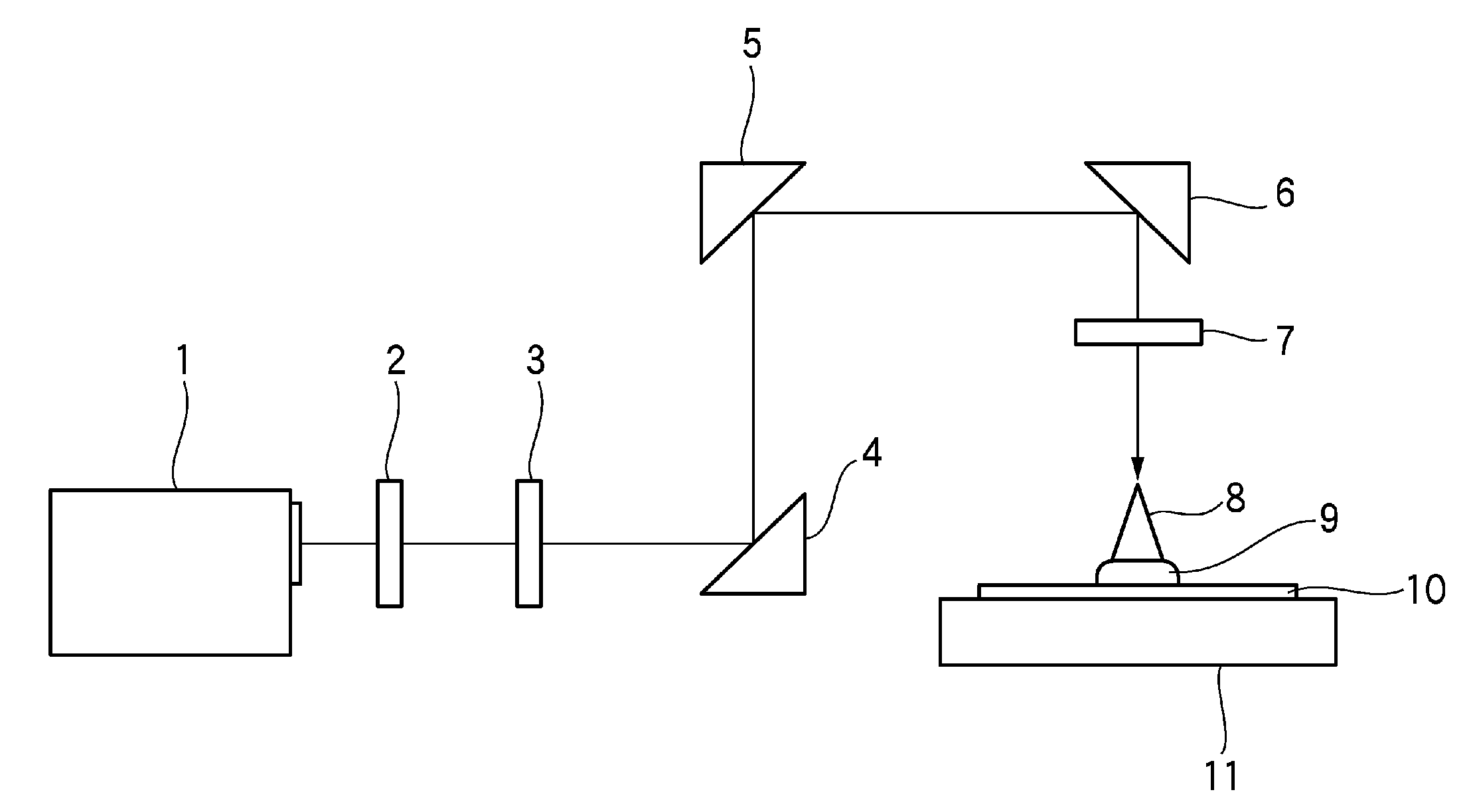
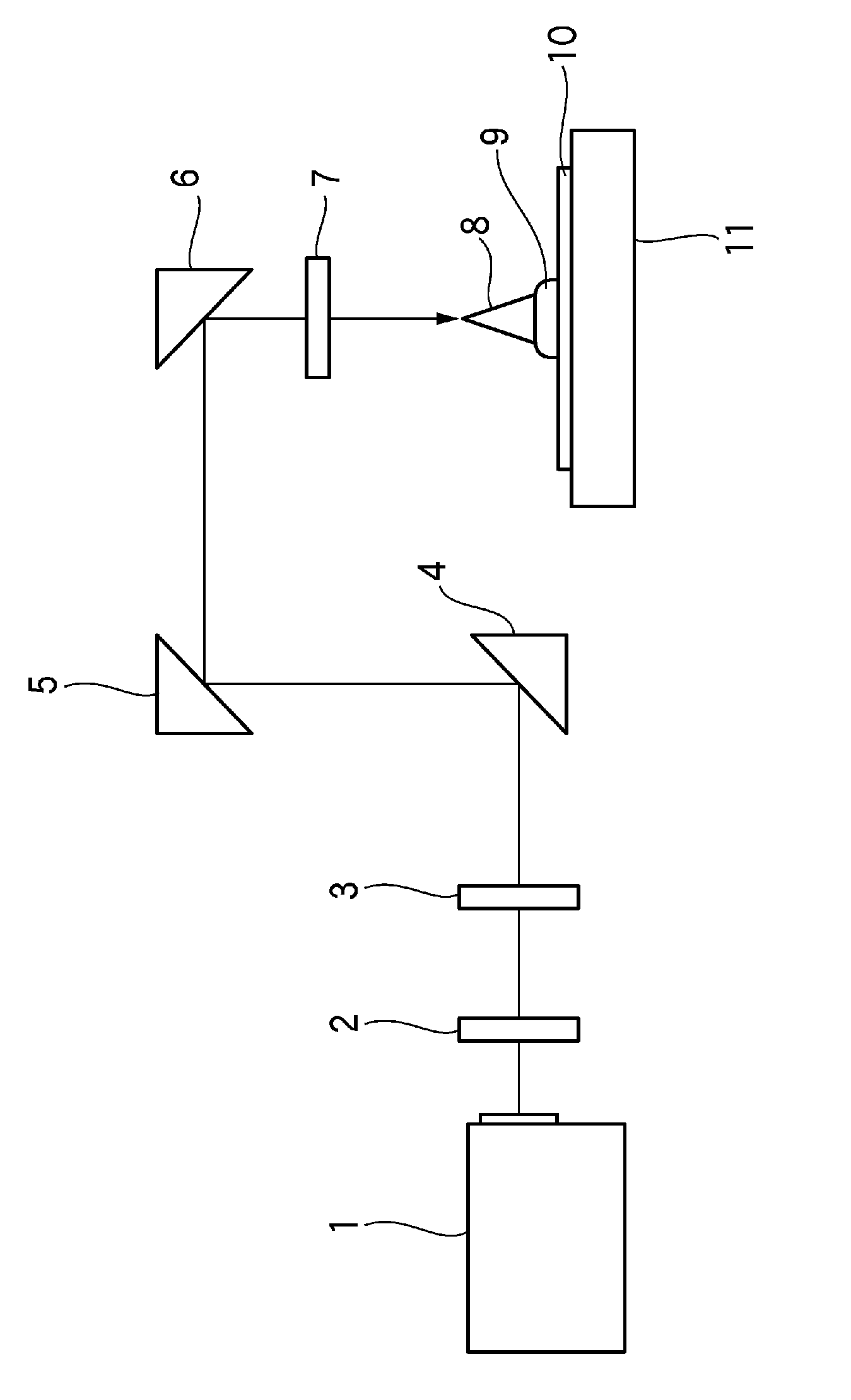
[0420]An organic antireflection film, ARC29A (produced by Nissan Chemical Industries, Ltd.), was coated on a silicon wafer and baked at 205° C. for 60 seconds to form a 78-nm antireflection film, and the positive resist solution prepared above was coated thereon and baked at 120° C. for 60 seconds to form a 160-nm resist film. The obtained wafer was exposed using an ArF excimer laser scanner (PAS5500 / 1100, manufactured by ASML, NA: 0.75, σo / σi: 0.85 / 0.55) and immediately after the exposure, heated (PEB) on a hot plat...

examples si-1

to SI-7 and Comparative Examples si-1 to si-5

(1) Formation of Lower Resist Layer

[0429]FHi-028DD Resist (resist for i-line, produced by Fujifilm Electronic Materials Co., Ltd.) was coated on a 6-inch silicon wafer by using a spin coater, Mark 8, manufactured by Tokyo Electron Ltd. and baked at 90° C. for 90 seconds to obtain a uniform film having a thickness of 0.55 μm. This film was further heated at 200° C. for 3 minutes to form a lower resist layer having a thickness of 0.40 μm.

(2) Formation of Upper Resist Layer

[0430]The components shown in Table 3 below were dissolved in a solvent to prepare a solution having a solid content concentration of II mass %, and this solution was microfiltered through a membrane filter having a pore size of 0.1 μm to prepare an upper resist composition.

[0431]This upper resist composition was coated on the lower resist layer in the same manner and heated at 130° C. for 90 seconds to form an upper resist layer having a thickness of 0.20 μm.

[0432]Resins ...


PUM


Abstract

A photosensitive composition contains: a compound capable of generating an acid upon irradiation with actinic rays or radiation; a basic compound represented by the formula (I-a) as defined herein; a basic compound represented by the formula (I-b) as defined herein; and a surfactant represented by the formula (II) as defined herein.

Description

FIELD OF THE INVENTION[0001]The present invention relates to a photosensitive composition for use in the production of a semiconductor such as IC, in the production of a circuit board for liquid crystal, thermal head and the like, and in other photofabrication processes, and a pattern forming method using the photosensitive composition. More specifically, the present invention relates to a photosensitive composition suitable for fine processing of a semiconductor device, where a short-wavelength light energy ray such as far ultraviolet ray, X-ray and electron beam is used, and a pattern forming method using the photosensitive composition.BACKGROUND OF THE INVENTION[0002]The chemical amplification resist composition is a pattern forming material capable of forming a pattern on a substrate by producing an acid in the exposed area upon irradiation with actinic rays or radiation such as far ultraviolet light and through a reaction using this acid as the catalyst, changing the solubility...

Claims


Application Information

Patent Timeline
IPC IPC(8): G03C1/06G03C5/00
CPCG03F7/0045G03F7/0046G03F7/0048G03F7/0382G03F7/0397G03F7/0758G03F7/094Y10S430/106Y10S430/115G03F7/0395
Inventor TSUBAKI, HIDEAKI
Owner FUJIFILM CORP
Why Eureka
Try Eureka