Mother/daughter switch design with self power-up control

Inactive Publication Date: 2008-10-30
TAIWAN SEMICON MFG CO LTD
View PDF4 Cites 20 Cited by
  • Summary
  • Abstract
  • Description
  • Claims
  • Application Information

AI Technical Summary

Benefits of technology

[0010]These and other problems are generally solved or circumvented, and technical advantages are generally achieved, by preferred embodiments of the present invention which provides a system and a method providing power to integrated circuitry with good power-on response time and reduced power-on transient glitches.
[0014]An advantage of a preferred embodiment of the present invention is the use of a dual switch design can allow for the optimization of the turn-on performance. For example, a small first switch (a daughter switch) can be used to meet electron migration performance requirements and a large second switch (a mother switch) can be used to meet performance requirements. The daughter switch can be turned on first to reduce a voltage difference across the switches and then the mother switch can be turned on to provide needed current. Since the voltage difference across the switches has been reduced, the magnitude of a resulting glitch is also reduced.
[0015]Yet another advantage of a preferred embodiment of the present invention is the reduced glitch that can occur when the mother switch is turned on. The reduction of the magnitude of the glitch can allow for the simultaneous turning on of multiple multi-voltage threshold design blocks. This can reduce the turn-on time of the multi-voltage threshold design blocks and improve the overall performance of the integrated circuit.
[0016]A further advantage of a preferred embodiment of the present invention is the self-monitored turn on of the mother switch. The mother switch can be automatically turned on, thereby minimizing a delay between the initiation of the turn-on of the multi-voltage threshold design block and the providing of the required current to the design block, which may occur if the turn on of the mother switch was base solely on a time delay.

Problems solved by technology

Without a concurrent change in process technology that can help reduce power consumption, an integrated circuit with an increased number of devices will tend to consume more power than an integrated circuit with fewer devices.
When in the sleep mode, the circuitry can consume a very small amount of power.
One disadvantage of the prior art technique of using a switch (either a header switch or a footer switch) to control the current path through a multi-voltage threshold design block is the sizing of the switch.
If the switch is large, to meet performance requirements, for example, then turning on the switch can cause a significant glitch.
On the other hand, if the switch is small, to meet electron migration requirements, for example, then the switch may not be able to provide adequate current to the multi-voltage threshold design block within timing requirements.

Method used


Image

  • Mother/daughter switch design with self power-up control
  • Mother/daughter switch design with self power-up control
  • Mother/daughter switch design with self power-up control

Examples


Embodiment Construction

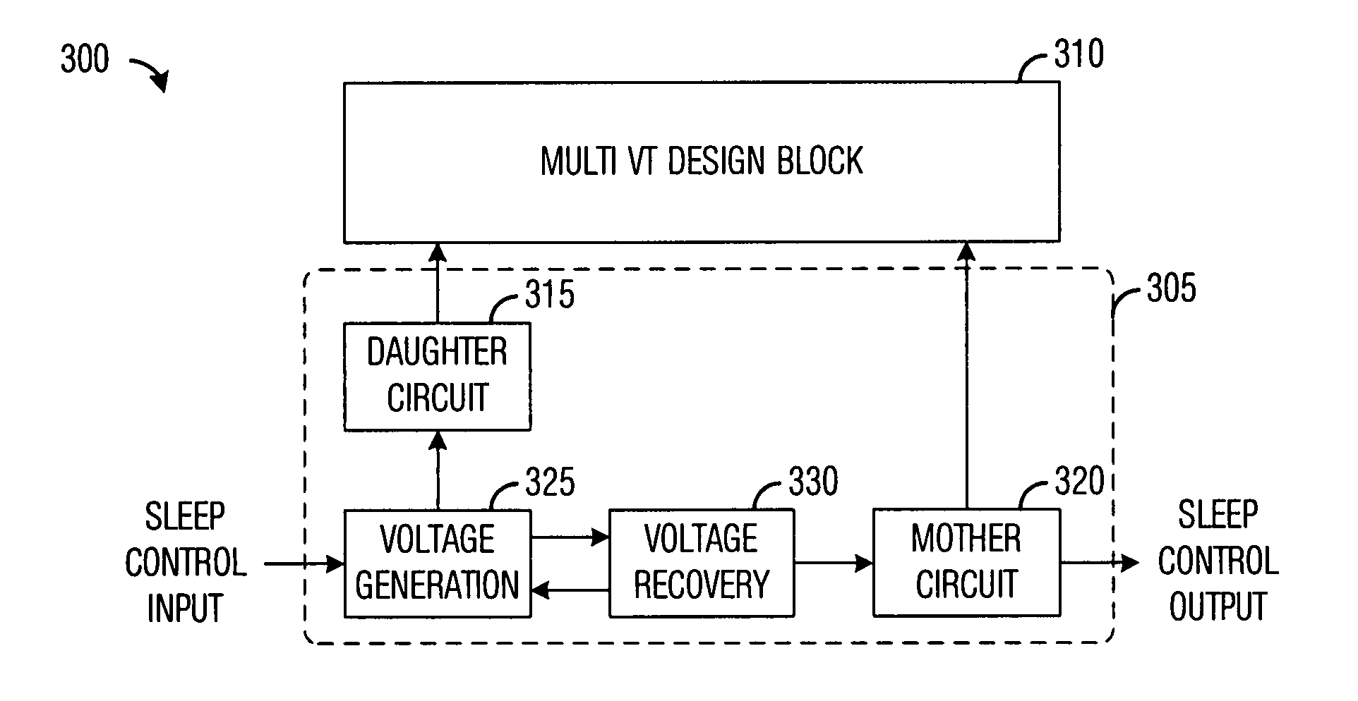
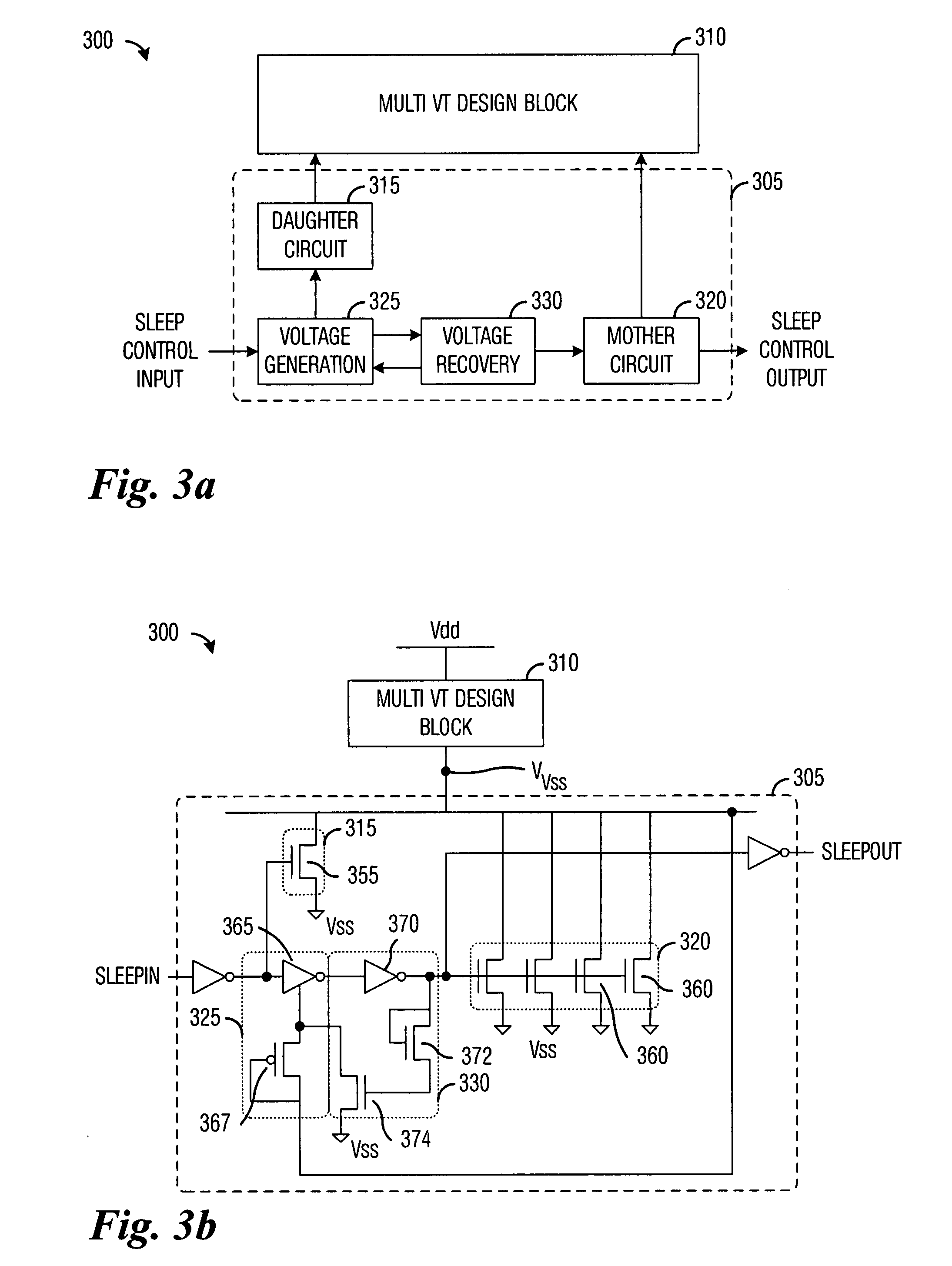
[0026]The making and using of the presently preferred embodiments are discussed in detail below. It should be appreciated, however, that the present invention provides many applicable inventive concepts that can be embodied in a wide variety of specific contexts. The specific embodiments discussed are merely illustrative of specific ways to make and use the invention, and do not limit the scope of the invention.

[0027]The present invention will be described with respect to preferred embodiments in a specific context, namely static random access memory (SRAM) ICs. The invention may also be applied, however, to other integrated circuits manufactured using complementary metal oxide semiconductor (CMOS) technologies and functional circuits of various types, such as processor ICs, controller ICs, application specific ICs, other types of memory ICs, and so forth. The present invention can be used where there is a desire to reduce power consumption by integrated circuits and / or rapidly awak...


PUM


Abstract

System and method for providing power to integrated circuitry with good power-on responsive time and reduced power-on transient glitches. A preferred embodiment comprises a daughter switch coupled to a circuit block, a first control circuit coupled to the daughter circuit, a second control circuit coupled to the first control circuit, and a mother circuit coupled to the circuit block and to the second control circuit. After the daughter switch is turned on by a control signal, the mother switch is not turned on until the daughter switch has discharged (charged) the voltage potential across power rails of the mother circuit to a point where glitches are minimized. The second control circuit turns on the mother circuit when the reduced voltage potential is reached, with a signal produced by the first control circuit reflects the voltage potential. Furthermore, a bypass circuit can be used to reduce leakage current.

Description

TECHNICAL FIELD[0001]The present invention relates generally to a system and a method for integrated circuits, and more particularly to a system and a method for providing power to integrated circuitry with good power-on response time and reduced power-on transient glitches.BACKGROUND[0002]There is a continued push by manufacturers of electronics to increase functionality of electronic devices. Greater functionality in an electronic device can provide additional processing power within the same package or increased convenience by reducing the total number of electronic devices. For example, rather than carrying a cellular telephone, a pager, and a personal digital assistant (PDA), a user can carry a single electronic device that has the combined functionality of the cellular telephone, the pager, and the PDA.[0003]Increasing the functionality of an electronic device can require the integration of additional electronics into the electronic device. Without a concurrent change in proce...

Claims


Application Information

Patent Timeline
IPC IPC(8): G06F1/32
CPCG06F1/3203
Inventor YANG, SHIH-HSIENWANG, CHUNG-HSINGLU, LEE-CHUNGTAI, CHUN-HUIHOU, CLIFF
Owner TAIWAN SEMICON MFG CO LTD
Why Eureka
Try Eureka