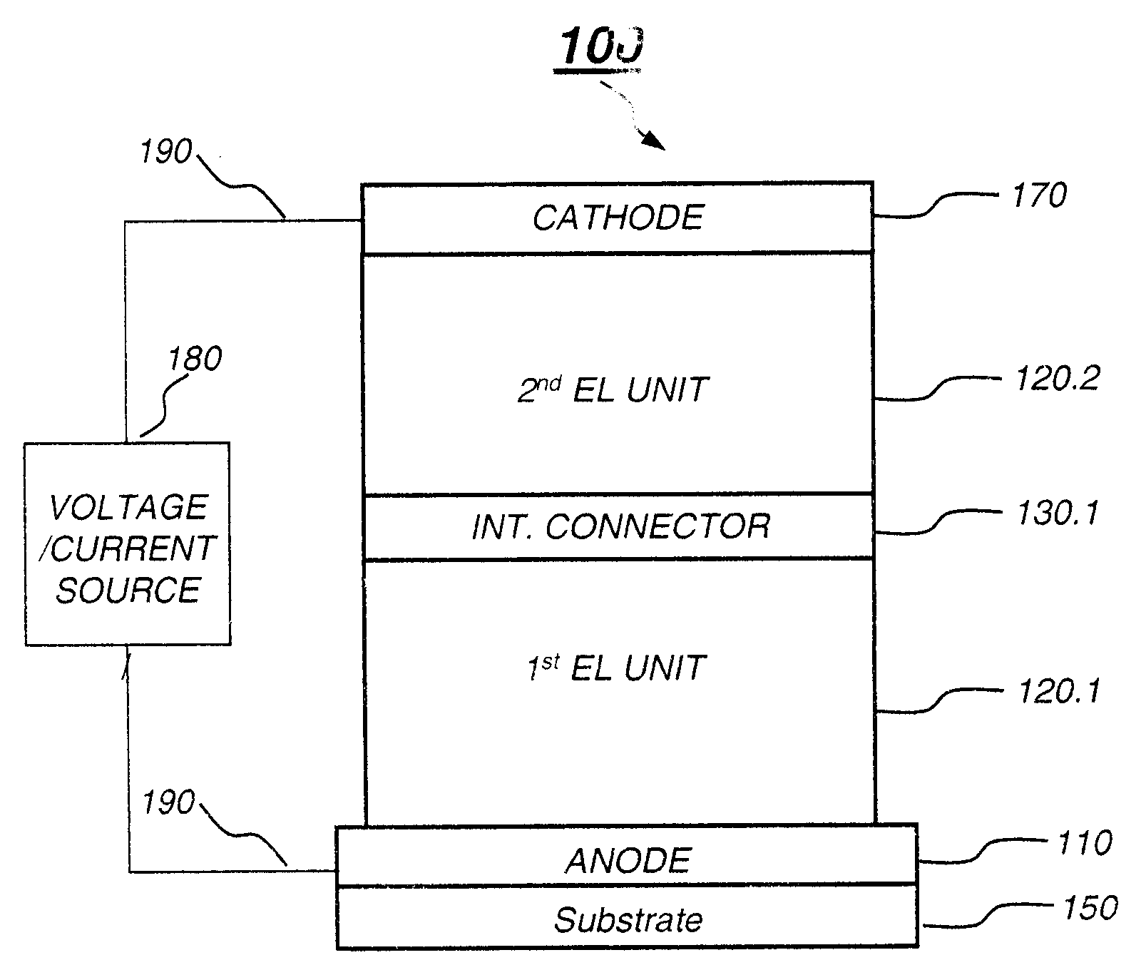
White light tandem OLED
a technology of white light and tandem oled, which is applied in the direction of energy-saving lighting, natural mineral layered products, sustainable buildings, etc., can solve the problems of low power efficiency, difficult to achieve light emission with strong intensity, and manufacturing difficulties, and achieves improved power efficiency, higher brightness, and long life.
- Summary
- Abstract
- Description
- Claims
- Application Information
AI Technical Summary
Benefits of technology
Problems solved by technology
Method used
Image
Examples
example 1-2
(Comparative) Single White EL Units
[0176]It is useful to begin with comparative OLEDs having only a single white EL unit. This makes the performance of tandem OLEDs having multiple EL units easier to understand.
example 1
Comparative
[0177]Over a clean glass substrate, an 85 nm thick indium tin oxide (ITO) was provided. The ITO surface was treated with a plasma oxygen etch, followed by plasma deposition of a 0.5 nm layer of a fluorocarbon polymer (CFx) as described in U.S. Pat. No. 6,208,075. The following layers were deposited over CFx layer in the following sequence by evaporation from heated boats under a vacuum of approximately 10−6 Torr:
[0178]a) a 240 nm thick HTL of NPB;
[0179]b) a 28 nm yellow light-emitting layer including 77% NPB (as host) with 3% yellow-orange emitting dopant as shown in Formula C7 and 20% anthracene derivative of formula AH3 as a stabilizer;
[0180]c) a 47 nm blue light-emitting layer including 92% AH3 host with 1% BEP (Formula F3) as blue-emitting dopant and 7% NPB;
[0181]d) a 10 nm thick ETL including ALQ; and
[0182]e) a cathode including 0.5 nm of LiF over the ETL to aid electron injection and 100 nm aluminum evaporated over the LiF.
[0183]The emission spectrum for the device...
example 2
Comparative
[0184]Over a clean glass substrate, an 85 nm thick indium tin oxide (ITO) was provided. The ITO surface was treated with a plasma oxygen etch, followed by plasma deposition of a 0.5 nm layer of a fluorocarbon polymer (CFx) as described in U.S. Pat. No. 6,208,075. The following layers were deposited over CFx layer in the following sequence by evaporation from heated boats under a vacuum of approximately 10−6 Torr:
[0185]a) a 240 nm HTL of NPB;
[0186]b) a red-orange light-emitting layer including 59.5% NPB (as host) with 40% Rubrene and 0.5% red emitting dopant (as shown in Formula A4);
[0187]c) a 20 nm blue light-emitting layer including 92% AH3 blue host with 1% BEP (Formula F3) as blue emitting dopant and 7% NPB;
[0188]d) a 15 nm green light-emitting layer including 49.75% AH3, 49.75% ALQ and 0.5% Formula D4 as green emitting dopant;
[0189]e) a 10 nm ETL ALQ; and
[0190]f) a cathode including 0.5 nm of LiF over the ETL to aid electron injection and 100 nm aluminum evaporated o...
PUM
| Property | Measurement | Unit |
|---|---|---|
| peak emission wavelength | aaaaa | aaaaa |
| peak emission wavelength | aaaaa | aaaaa |
| peak emission wavelength | aaaaa | aaaaa |
Abstract
Description
Claims
Application Information
 - R&D
- Intellectual Property
- Life Sciences
- Materials
- Tech Scout
- Unparalleled Data Quality
- Higher Quality Content
- 60% Fewer Hallucinations
Browse by: Latest US Patents, China's latest patents, Technical Efficacy Thesaurus, Application Domain, Technology Topic, Popular Technical Reports.
© 2025 PatSnap. All rights reserved.Legal|Privacy policy|Modern Slavery Act Transparency Statement|Sitemap|About US| Contact US: help@patsnap.com


