
Non-rectangular display apparatus

a display apparatus and non-rectangular technology, applied in the direction of static storage, digital storage, instruments, etc., can solve the problems of no reference to the position relationship, the non-rectangular display apparatus of a narrow frame edge width is difficult to implement, and the problem of seriousness similar to that referred to above, etc., to achieve the effect of reducing interferen

Active Publication Date: 2008-10-30
TIANMA MICRO ELECTRONICS CO LTD
View PDF4 Cites 128 Cited by
  • Summary
  • Abstract
  • Description
  • Claims
  • Application Information

AI Technical Summary

Benefits of technology

[0045]According to the present invention, it is possible to construct a display apparatus of a narrower frame edge width having a non-rectangular shape analogous with the non-rectangular display surface. It is because the signal line driving circuit may be laid out to a narrower width by elongating the signal line driving circuit having a larger number of active elements that make up the circuit and thus having a larger circuit size.
[0047]According to the present invention, it is possible to reduce the interference between the scan lines or between the signal lines. The reason is that the active matrix may be connected to the scan line driving circuit or to the signal line driving circuit by bending the scan line or the signal line without changing the relative distance therebetween.
[0049]According to the present invention, driving circuits may be arranged with higher density in a display apparatus having a non-rectangular display surface, so that it is possible to produce a display apparatus of a narrow frame edge width from a substrate and apparatus both of which are non-rectangular in shape.
[0050]The reason is that the driving circuit arranged adjacent to the display section are arrayed along the outer circumference of the non-rectangular display section, from one group of circuit units having the common function to another. This enables the non-rectangular driving circuits to be laid out to higher density to provide for a narrow frame edge width of the display apparatus with the shape and the size of the substrate of the apparatus proximate to those of the display section.
[0051]According to the present invention, there is no necessity of using a special dicing equipment to slice out the non-rectangular driving circuit or adding a special process to produce the non-rectangular display apparatus with a narrow frame edge width. The reason is that, since the active elements constituting the driving circuit are produced on the same substrate and using the same process to produce the active elements of the active matrix, it is possible to co-use the manufacturing equipment and the process for manufacturing the driving circuit.

Problems solved by technology

Hence, the non-rectangular display apparatus of a narrow frame edge width is difficult to implement.
The problem similar to that referred to above becomes serious in case the driving circuit is arrayed in proximity to the circular rim.
However, no reference has been made to the position relationship between the gate lines and the data lines that make up the liquid crystal panel and the liquid crystal driving circuit that drives the gate and data lines.
That is, there lacks the disclosure as to specified means for implementing high density mounting of the liquid crystal driving circuit.
However, in such case, driving circuits, typified by a scan line driving circuit and signal line driving circuit, pose a problem.
A rectangular driving circuit, such as a semiconductor IC mounted on a substrate of a display apparatus, as disclosed in Patent Document 1 (WO93 / 004460A1), for example, the substrate has corners, and hence the apparatus cannot afford a narrow frame edge width.

Method used


Image

  • Non-rectangular display apparatus
  • Non-rectangular display apparatus
  • Non-rectangular display apparatus

Examples


first exemplary embodiment

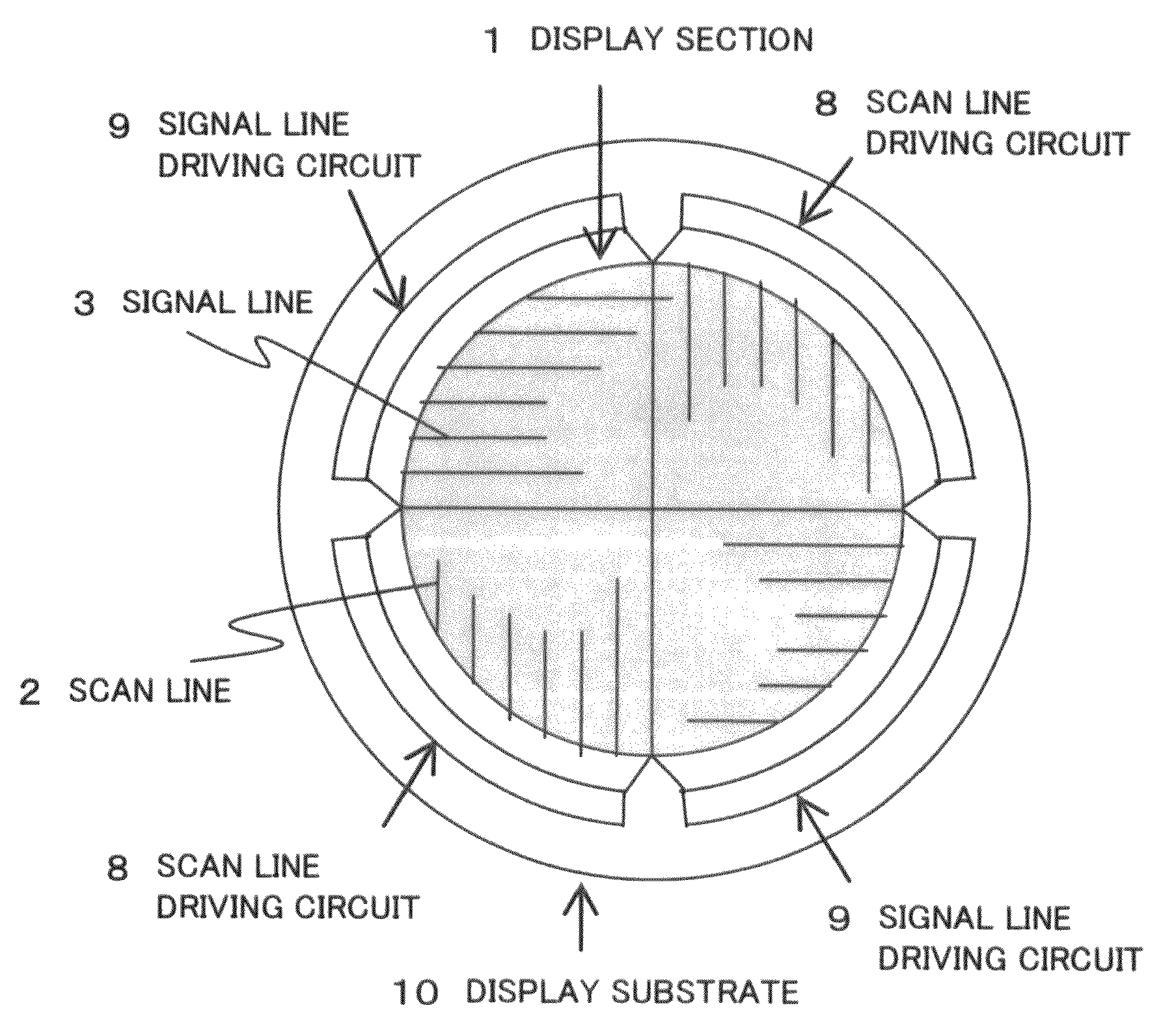
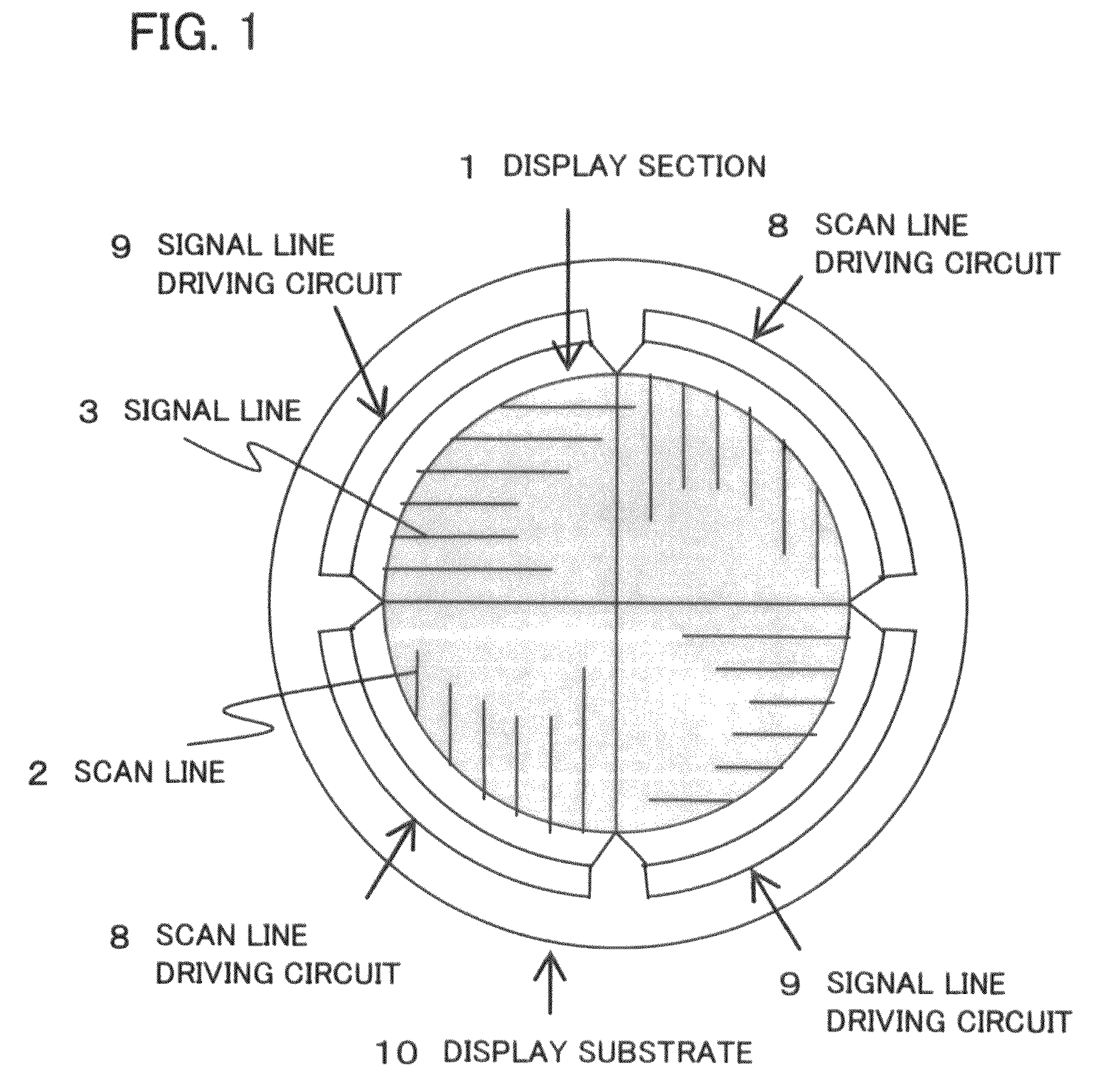
[0084]FIG. 1 is a plan view showing the configuration of an exemplary embodiment of the present invention. The present exemplary embodiment is directed to a non-rectangular display apparatus having a circular-shaped display section 1. The display apparatus of the present exemplary embodiment includes an active matrix display section 1, two scan line driving circuits 8 and two signal line driving circuits 9, each being formed on a display substrate 10. The active matrix display section 1 includes a plurality of scan lines 2, a plurality of signal lines 3, and a plurality of pixels and active elements formed of thin-film transistors, arranged at the intersections of the scanning and signal lines. The scan line driving circuit 8 is formed by thin-film transistors, and the signal line driving circuit 9 is formed by thin-film transistors.

[0085]By having both the scan line driving circuits 8 and the signal line driving circuits 9 formed to a planar sector shape of a curvature that conform...

second exemplary embodiment

[0125]FIG. 9 shows the layout of a second exemplary embodiment of the present invention. In the present exemplary embodiment, the shift registers 100, which are repeatedly translated in the X- and Y-directions, as shown in FIG. 7, are also tilted at an optional angle.

[0126]By so doing, the shift registers 100 may be arranged in the vicinity of the rim part of the display section 1. The power supply lines VH, VL, clock signal lines CLK1, CLK2 and the interconnecting output lines obliquely interconnect the respective shift registers 100, with the shortest path lengths, for instance.

[0127]In the present exemplary embodiment, the distance or spacing along the X-direction between the shift registers 100 is equal to that between the neighboring scan lines 2. That is, distance or spacing along the X-direction is constant. However, the distance or spacing along the Y-direction and the pitch of the angle of rotation are changed.

[0128]By optionally determining the distance or spacing along th...

third exemplary embodiment

[0130]FIG. 10 shows an example of the layout of a third exemplary embodiment of the present invention. In the present exemplary embodiment, the shift registers, tilted at an optional angle, may be allowed to extend along the rim of the display section 1, and the respective shift registers are arrayed with a narrower pitch.

[0131]That is, rectangular shift register 100 (FIG. 3) are placed closer to one another such that the respective corners of the neighboring shift register 100 touch each other. By so doing, it is possible to reduce the length of the scan line driving circuit 8 in its entirety.

[0132]If the same length of a part of the rim of the display section 1 as that of FIG. 7 or 9 is taken up by the scan line driving circuit 8, the layout width of each shift register 100 may be set to a larger value.

[0133]With the same circuit size, the layout height of the shift register 100 may be correspondingly reduced. It is because the scan line driving circuit 8 becomes narrower in width...


PUM


Abstract

Disclosed is a display apparatus comprising an active matrix display section including a plurality of signal lines and scan lines, arranged in a matrix on a substrate, and a plurality of pixels and active elements arranged at intersections of the signal and scan lines, a scan line driving circuit for driving the scan lines and a signal line driving circuit for driving the signal lines. The display section has a non-rectangular shape. The active elements that make up the scan line driving circuit and / or the signal line driving circuit are formed by the same manufacturing process as that for forming the active elements in the active matrix display section. The scan line driving circuit and / or the signal line driving circuit are each a set of circuit units having the same function. These circuit units are arranged to conform to and extend around the outer circumference of the non-rectangular display section.

Description

REFERENCE TO RELATED APPLICATION[0001]The present application is claiming the priority of the earlier Japanese patent applications No. 2007-118912 filed on Apr. 27, 2007 and No. 2008-106654 filed on Apr. 16, 2008, the entire disclosure thereof being incorporated herein by reference thereto.FIELD OF THE INVENTION[0002]This invention relates a display apparatus having a non-rectangular display section.BACKGROUND OF THE INVENTION[0003]FIG. 24 is a diagram schematically illustrating a typical configuration of a conventional active matrix display apparatus. Referring to FIG. 24, a pixel and an active element, such as a thin-film transistor, are provided at an intersection of a signal line and a data line arranged in a matrix pattern relative to each other. During the time a selection pulse is supplied to a scan line, the active element, the gate terminal of which is connected to the scan line, is in an on-state. Hence, the signal potential, charged to the signal line, is applied to a pix...

Claims


Application Information

Patent Timeline
IPC IPC(8): G09G3/20
CPCG09G3/20G09G2300/0426G09G2310/0267G09G2310/0275G09G2310/0286G11C19/28G09G2310/0281H10K59/131
Inventor NONAKA, YOSHIHIRO
Owner TIANMA MICRO ELECTRONICS CO LTD
Learn More