Semiconductor Light Emitting Device and Method for Manufacturing the Same

Inactive Publication Date: 2008-10-23
ROHM CO LTD
View PDF0 Cites 3 Cited by
  • Summary
  • Abstract
  • Description
  • Claims
  • Application Information

AI Technical Summary

Benefits of technology

[0016]By the present invention, since the Al layer is formed as one side of the n-side electrode, which is a side connected to the n-type layer made of the nitride semiconductor, the contact resistance with the nitride semiconductor layer is significantly smaller than that with Ti and the n-side electrode in which a driving voltage is not raised can be formed.
[0017]Since the barrier metal layer made of a material having a higher melting temperature than that of Al is formed, while the Au layer is formed on the surface through a barrier metal layer to improve adhesion property of wire bonding, the Au layer on the surface is not damaged even in the heat treatment for obtaining the ohmic contact of the Al layer and the nitride semiconductor layer after forming all of metal layers for the n-side electrode, because the barrier metal layer can prevent the Al layer and the Au layer from alloying. Then, the Au layer can be left on the surface of the metal layers as it is, while the ohmic contact can be obtained by diffusing Al into the nitride semiconductor layer by sintering (heat treatment). With a simple process, an electrical connection with a gold wire or the like for wire bonding can be performed surely and with a low contact resistance, and consequently, an electrical connection with the nitride semiconductor layer can be performed in a remarkably low resistance.

Problems solved by technology

At this sintering, as Ti, Al and Au make an alloy if an Au layer is already formed, it becomes useless to form the Au layer because a part of alloyed Al is exposed on the surface.
Then, as it is necessary to form a Ti / Au layer or an Au layer further after sintering a Ti layer and an Al layer after laminating them, there rises a problem such that a manufacturing process becomes complicated because a depositing process of layer(s) should be applied twice.

Method used


Image

  • Semiconductor Light Emitting Device and Method for Manufacturing the Same
  • Semiconductor Light Emitting Device and Method for Manufacturing the Same
  • Semiconductor Light Emitting Device and Method for Manufacturing the Same

Examples


Embodiment Construction

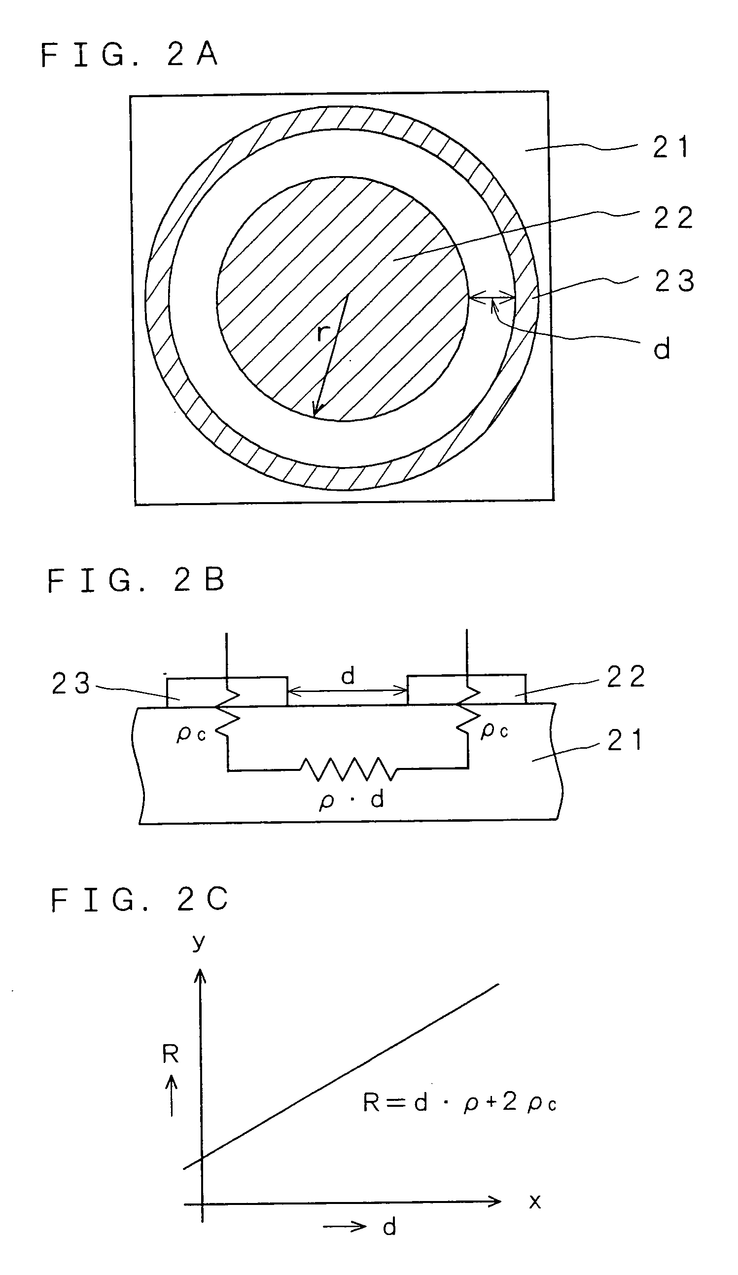
[0035]An explanation will be given below of a semiconductor light emitting device according to the present invention in reference to the drawings. In FIG. 1, there is shown a cross-sectional view explaining an embodiment of the semiconductor light emitting device according to the present invention, in which nitride semiconductor layers suitable for emitting a blue type light are laminated on a sapphire substrate.

[0036]As shown in FIG. 1, in the semiconductor light emitting device according to the present invention, semiconductor layers 2 to 8 to form a light emitting layer are laminated on a surface of a substrate 1 made of, for example, a sapphire (Al2O3 single crystal) or the like and a p-side electrode 10 is formed on the surface thereof thorough a light transmitting conductive layer 9. An n-side electrode 11 is formed on an exposed surface of an n-type layer 4, exposed by removing a part of the semiconductor layers 4 to 8 by etching. The present invention is characterized in tha...


PUM


Abstract

There is provided a semiconductor light emitting semiconductor device including an n-side electrode which has a structure capable of stably suppressing the contact resistance between the n-side electrode and a nitride semiconductor layer. Further, there is provided a light emitting device and a manufacturing method wherein an ohmic contact between the n-side electrode and the nitride semiconductor layer can be obtained by a simple manufacturing process, and the n-side electrode has an Au layer on a top surface to facilitate wire bonding. Semiconductor layers (2-8) to form a light emitting layer are laminated on a surface of a substrate (1) made of, for example, a sapphire (Al2O3 single crystal) or the like and a p-side electrode (10) is formed on the surface thereof thorough a light transmitting conductive layer (9). An n-side electrode (11) is formed on an exposed surface of an n-type layer (4), exposed by removing a part of the semiconductor layers (4-8) by etching. The n-side electrode includes actually an Al layer (11a) in contact with the n-type layer, a barrier metal layer (11b) and an Au layer (11c).

Description

FIELD OF THE INVENTION[0001]The present invention relates to a semiconductor light emitting device emitting a blue type light (which means a light having a color band from ultraviolet to yellow), in which a nitride semiconductor is laminated on a substrate, and relates to a method for manufacturing the same. More particularly, the present invention relates to a nitride semiconductor light emitting device which can be formed in a little production manhour and easily, while improving an ohmic contact of an n-side electrode formed on an n-type layer of the nitride semiconductor, and relates to a method for manufacturing the same.BACKGROUND OF THE INVENTION[0002]In the prior art, a semiconductor light emitting device emitting a blue type light is formed, for example, on a sapphire substrate by laminating an n-type layer made of GaN or the like, an active layer (light emitting layer) made of a material having a smaller band gap energy than that of the n-type layer and deciding a waveleng...

Claims


Application Information

Patent Timeline
IPC IPC(8): H01L33/00H01L33/32H01L33/40
CPCH01L33/32H01L33/40
Inventor SAKAI, MITSUHIKOKOHDA, SHINICHISONOBE, MASAYUKINAKAHARA, KEN
Owner ROHM CO LTD
Why Eureka
Try Eureka