Tunneling magnetic sensor including free magnetic layer and magnesium protective layer disposed thereon and method for manufacturing tunneling magnetoresistive sensor
- Summary
- Abstract
- Description
- Claims
- Application Information
AI Technical Summary
Benefits of technology
Problems solved by technology
Method used
Image
Examples
examples
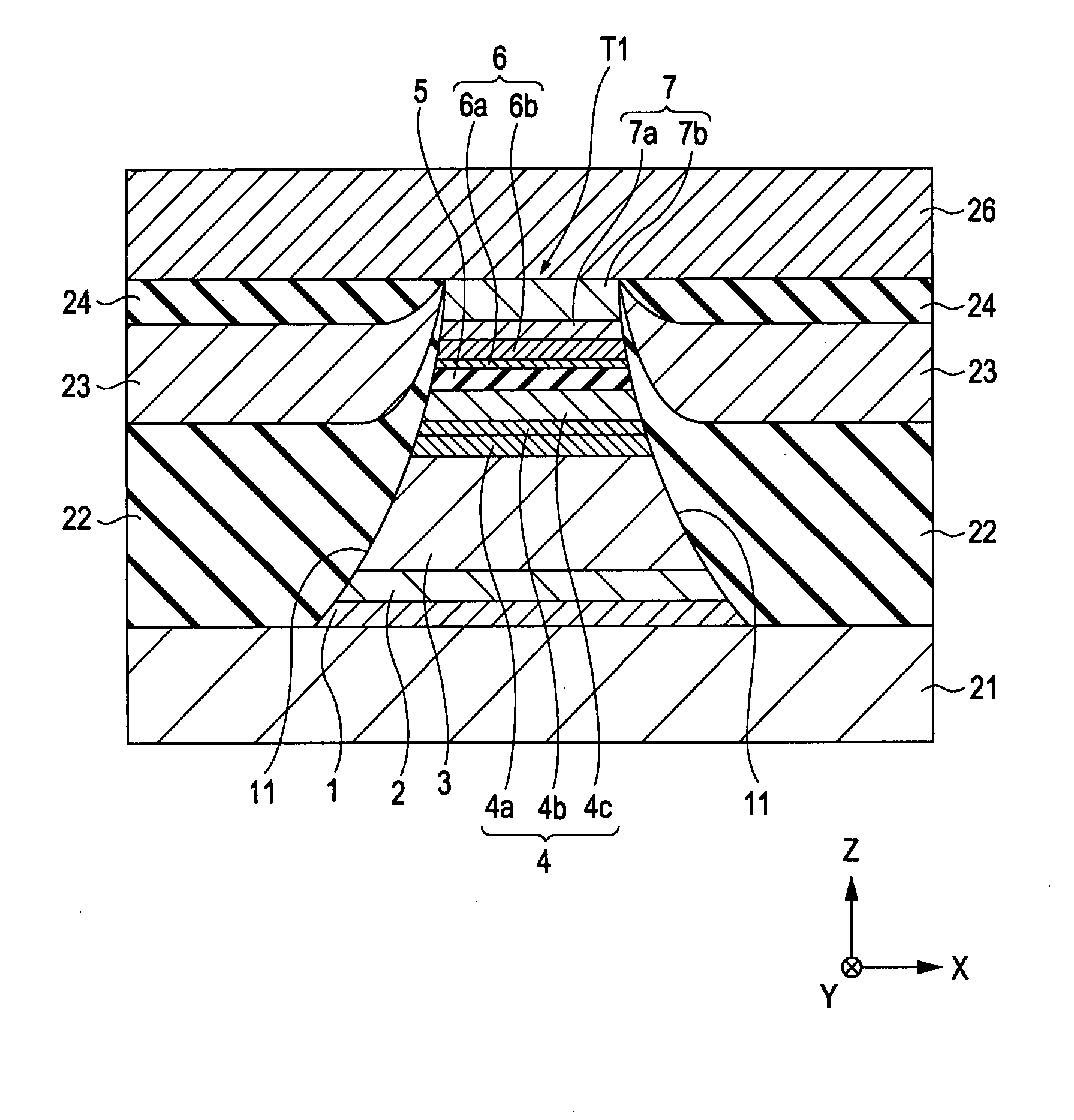
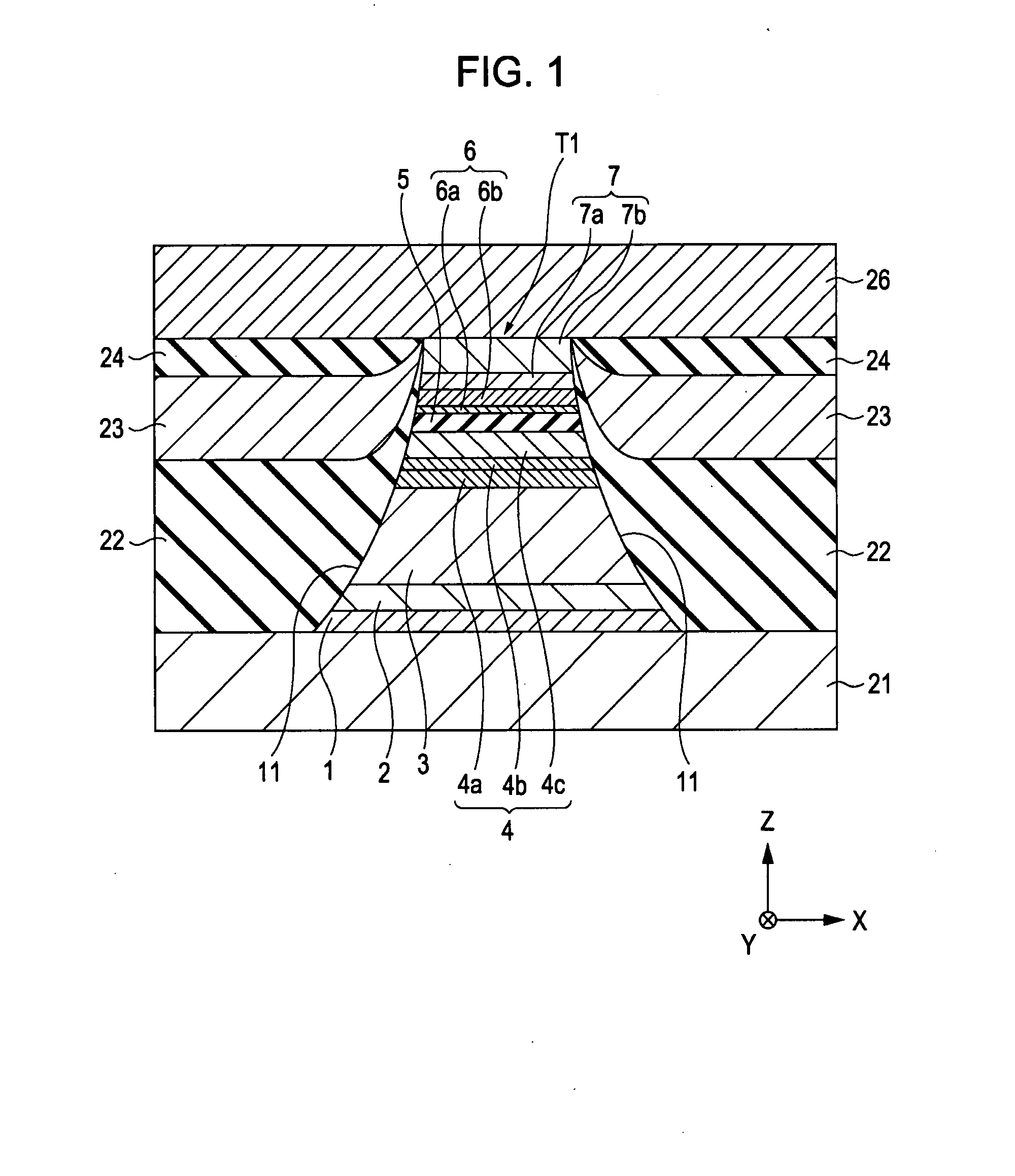
[0095]Tunneling magnetic sensors were prepared so as to have configurations similar to the configuration of the tunneling magnetic sensor shown in FIG. 1.
[0096]In Example 1, a tunneling magnetic sensor including an insulating barrier layer 5 made of Al—O was prepared as described below.
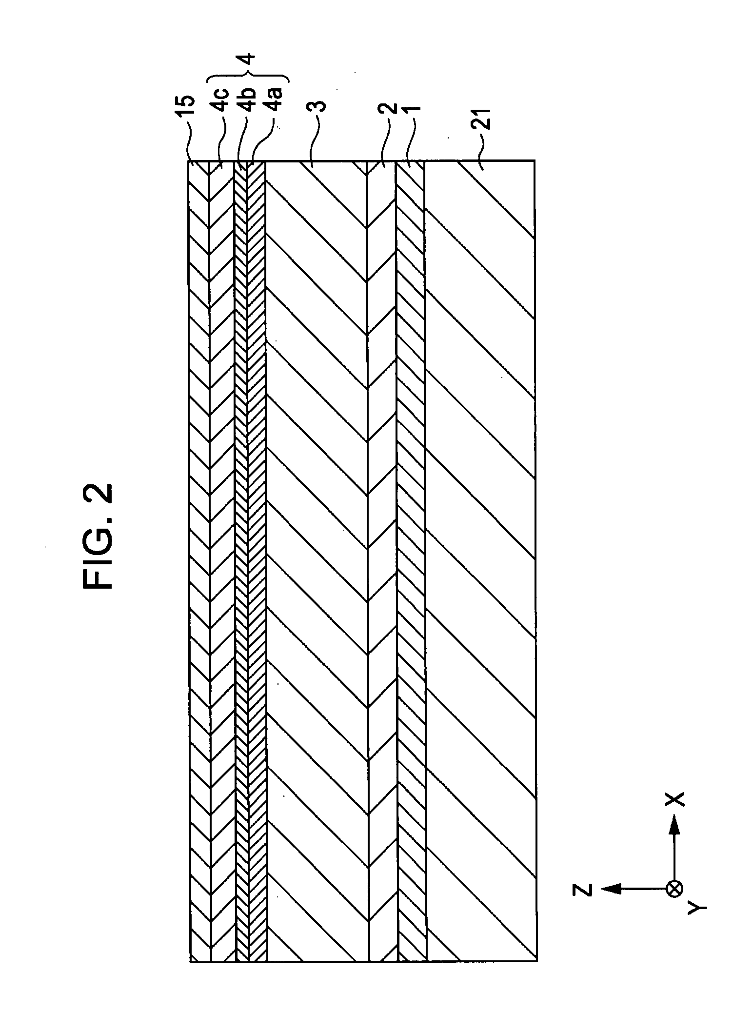
[0097]The following layers were deposited on a lower shield layer 21 in this order: a base layer 1, made of Ta, having an average thickness of about 80 Å; a seed layer 2, made of a Ni—Fe—Cr alloy, having an average thickness of about 50 Å; an antiferromagnetic layer 3, made of an Ir—Mn alloy, having an average thickness of about 70 Å; a pinned magnetic layer 4 including a first pinned magnetic sublayer 4a which contained about 70 atomic percent Co and 30 atomic percent Fe and which had an average thickness of about 14 Å, a non-magnetic intermediate sublayer 4b which was made of Ru and which had an average thickness of about 9.1 Å, and a second pinned magnetic sublayer 4c which contained about 60 atomi...
PUM
 Abstract
Description
Claims
Application Information
 - R&D
- Intellectual Property
- Life Sciences
- Materials
- Tech Scout
- Unparalleled Data Quality
- Higher Quality Content
- 60% Fewer Hallucinations
Browse by: Latest US Patents, China's latest patents, Technical Efficacy Thesaurus, Application Domain, Technology Topic, Popular Technical Reports.
© 2025 PatSnap. All rights reserved.Legal|Privacy policy|Modern Slavery Act Transparency Statement|Sitemap|About US| Contact US: help@patsnap.com


