Eureka AIR delivers breakthrough ideas for toughest innovation challenges, trusted by R&D personnel around the world.

Voltage-clamping device and operational amplifier and design method thereof

Inactive Publication Date: 2008-10-16
RAYDIUM SEMICON
View PDF2 Cites 9 Cited by
  • Summary
  • Abstract
  • Description
  • Claims
  • Application Information

AI Technical Summary

Benefits of technology

[0009]The invention is directed to a voltage-clamping device and an operational amplifier using the same capable of effectively resolving the disadvantages of high substrate current, having ill effects of hot electrons, latchup and snapback, short lifespan, and higher and power consumption encountered in the conventional operational amplifier. The invention substantially reduces the ill effects caused due to high substrate current, and enables the operational amplifier and the analog circuit using the same to have the advantages of longer lifespan, lower power consumption, and longer battery life.
[0010]According to a first aspect of the present invention, a voltage-clamping device used in an operational amplifier is provided. The operational amplifier comprises a first transistor. The cross-voltage between the gate and the source of the first transistor is near to a specific voltage and the cross-voltage between the drain and the source of the first transistor is not equal to zero, so as to generate a big substrate current. The voltage-clamping device comprises a second transistor whose source and gate are respectively coupled to the drain of the first transistor and used for receiving a bias signal, so that the second transistor is biased in saturation region, and the voltage at the source of the second transistor is made equal to the difference between the bias signal and the threshold voltage of the second transistor. Thus, the cross-voltage between the drain and the source of the first transistor is reduced so as to reduce the substrate current accordingly.
[0011]According to a second aspect of the present invention, an operational amplifier comprising an input stage circuit and an output stage circuit is provided. The input stage circuit is for receiving a differential signal, so as to generate an intermediate signal accordingly. The output stage circuit is for generating an output signal in response to intermediate signal. The output stage circuit comprises a first and a second transistor. The cross-voltage between the gate and the source of the first transistor is near to a specific voltage, and the cross-voltage between the drain and the source of the first transistor is not equal to zero, so as to generate a big substrate current. The source of the second transistor is coupled to the drain of the first transistor, and the gate of the second transistor receives a bias signal, so that the second transistor is biased in saturation region, and the voltage at the source of the second transistor is made equal to the difference between the bias signal and the threshold voltage of the second transistor. Thus, the cross-voltage between the drain and the source of the first transistor is reduced so as to reduce the substrate current of the first transistor accordingly.

Problems solved by technology

A part of hot electrons flow to the gate of the transistor and is trapped in the gate oxidation layer, causing the threshold voltage, saturation current and the characteristic of the transistor to change with the using time and end up with malfunction.
As a result, the conventional operational amplifier and the source driver using the same have the disadvantage of shorter lifespan.
As higher substrate current would also increase the working current of the direct current of the conventional operational amplifier and the source driver using the same, the conventional operational amplifier and the conventional source driver using the same have the disadvantage of high power consumption.
When the conventional operational amplifier and the conventional source driver using the same are used in portable products, the portable products will have poor battery life.
As a result, the substrate current increases drastically and more hot electrons are generated, and the above disadvantages are made even worse.

Method used


Image

  • Voltage-clamping device and operational amplifier and design method thereof
  • Voltage-clamping device and operational amplifier and design method thereof
  • Voltage-clamping device and operational amplifier and design method thereof

Examples


Embodiment Construction

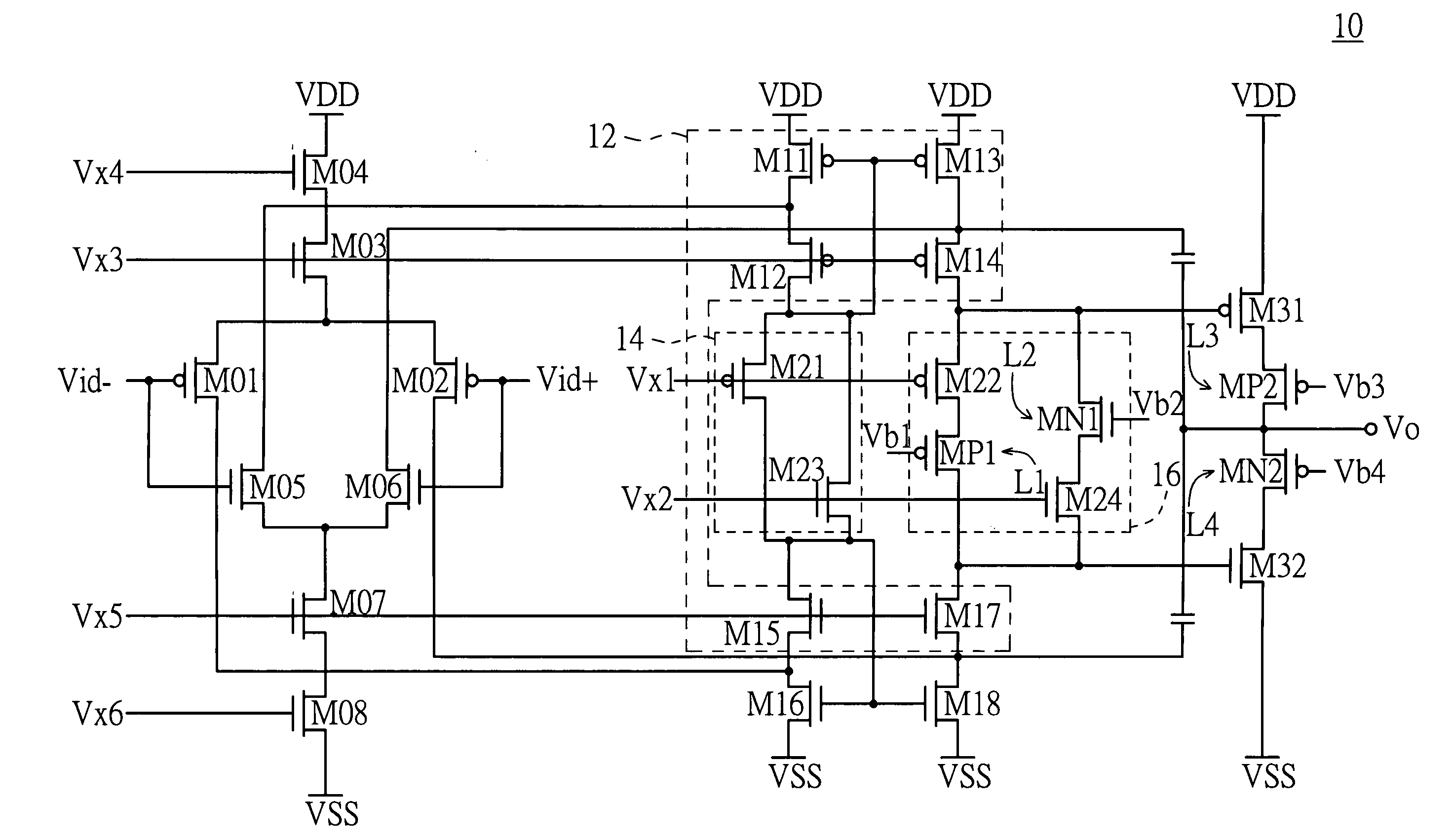
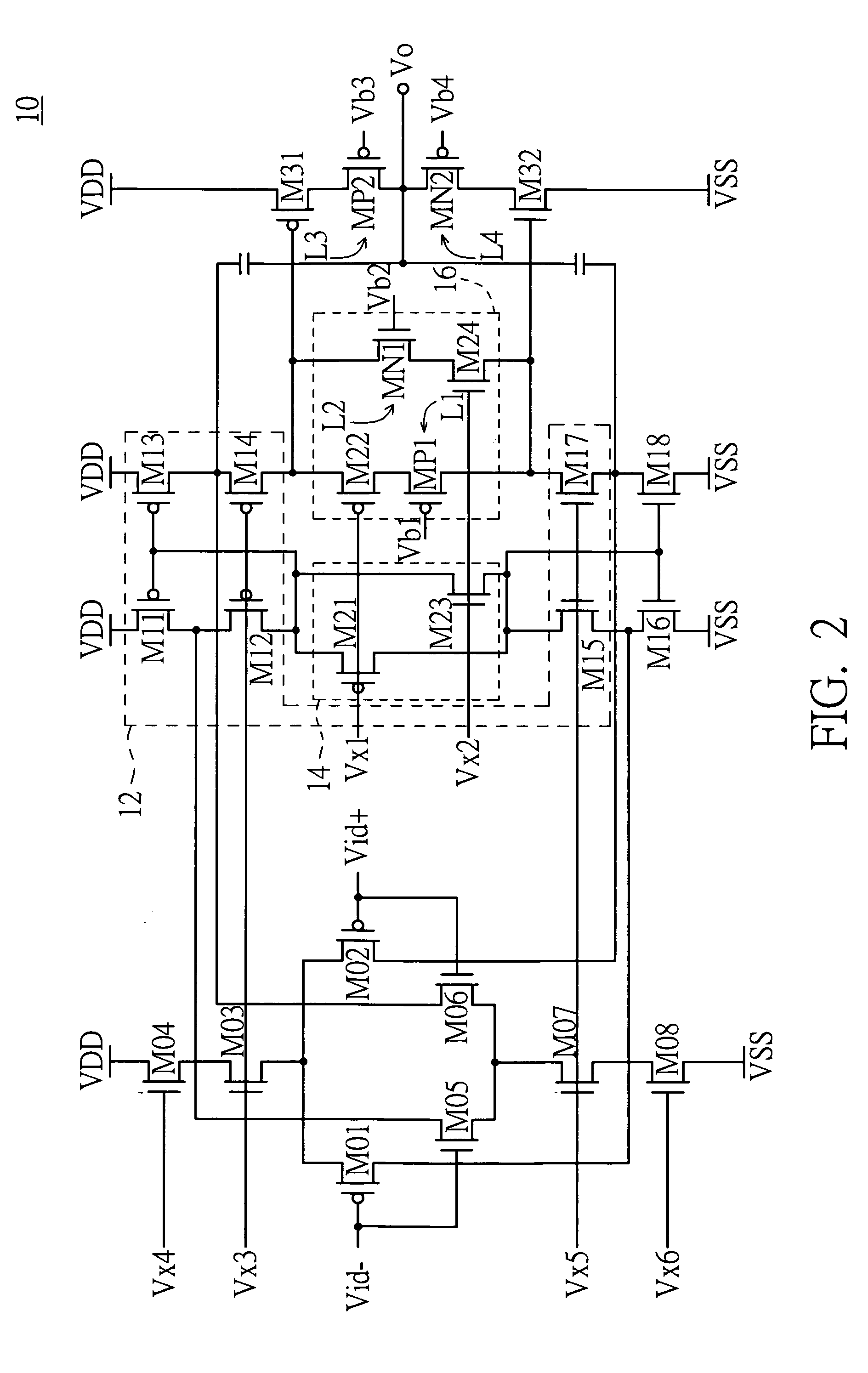
[0018]Referring to FIG. 2, a circuit diagram of an operational amplifier according to a first embodiment of the invention is shown. In the present embodiment of the invention, the operational amplifier 10 is exemplified by a two-stage rail-to-rail I / O operational amplifier. The operational amplifier 10 comprises an input stage circuit and an output stage circuit. The input stage circuit is a rail-to-rail input circuit for receiving two differential input signals Vid+ and Vid− and generating four intermediate signals Vc1˜Vc4 according to the differential input signals Vid+ and Vid−. The output stage circuit is a rail-to-rail class AB output circuit for providing an output signal Vo in response to the intermediate signals Vc1˜Vc4.

[0019]The input stage circuit comprises four input transistors M01, M02, M05 and M06, wherein the input transistors M01 and M02 are both P-type metal oxide semiconductor (PMOS) transistors, and the input transistors M05 and M06 are both N-type metal oxide sem...


PUM


Abstract

A voltage-clamping device used in an operational amplifier is provided. The operational amplifier comprises a first transistor. The cross-voltage between the gate and the source of the first transistor is near to a specific voltage and the cross-voltage between the drain and the source of the first transistor is not equal to zero, so as to generate a big substrate current. The voltage-clamping device comprises a second transistor whose source and gate are respectively coupled to the drain of the first transistor and used for receiving a bias signal, so that the second transistor is biased in saturation region, and the voltage at the source of the second transistor is made equal to the difference between the bias signal and the threshold voltage of the second transistor. Thus, the cross-voltage between the drain and the source of the first transistor is reduced and the substrate current is reduced accordingly.

Description

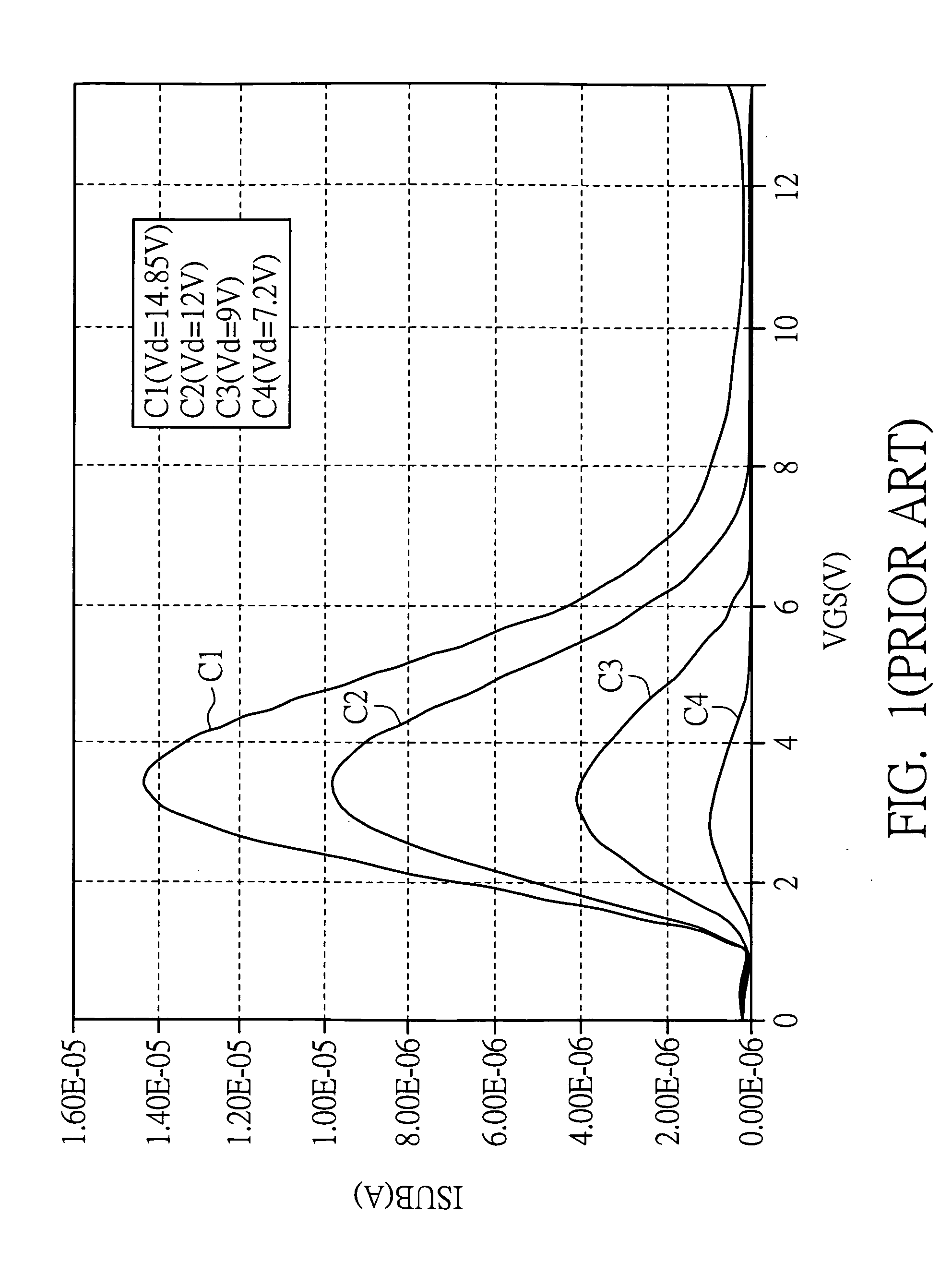
[0001]This application claims the benefit of Taiwan application Serial No. 096112595, filed APR. 10, 2007, the subject matter of which is incorporated herein by reference.BACKGROUND OF THE INVENTION[0002]1. Field of the Invention[0003]The invention relates in general to a voltage-clamping device, and more particularly to a voltage-clamping device capable of reducing the substrate current and negative effects generated in a transistor of an operational amplifier.[0004]2. Description of the Related Art[0005]Liquid crystal display comprises a source driver, a gate driver and a liquid crystal display panel, wherein the liquid crystal display panel has a pixel array. The source driver provides pixel data to columns of the pixel array and the gate driver turns on corresponding rows of the pixel array to display the desired image. Referring to FIG. 1, a curve of bias voltage vs. substrate current of a transistor of an operational amplifier is shown. According to most conventional technolog...

Claims


Application Information

Patent Timeline
IPC IPC(8): H03F3/45
CPCH03F3/3022H03F3/45183H03F3/45219H03F2203/30015H03F2203/30084H03F2203/30117H03F2203/45134H03F2203/45626H03F2203/45636
Inventor TSO, KO-YANGLIN, KEH-LALIANG, YANN-HSIUNGCHAO, CHIN-CHIEH
Owner RAYDIUM SEMICON
Why Eureka
Eureka Blog
Learn More