Scanning electron microscope and method for processing an image obtained by the scanning electron microscope
a scanning electron microscope and scanning electron technology, applied in the field of scanning electron microscopes, can solve the problems of insufficient improvement of the resolving power due to the beam intensity distribution, and the inability to reduce the resolving power of the region out of focus,
- Summary
- Abstract
- Description
- Claims
- Application Information
AI Technical Summary
Benefits of technology
Problems solved by technology
Method used
Image
Examples
embodiment 1
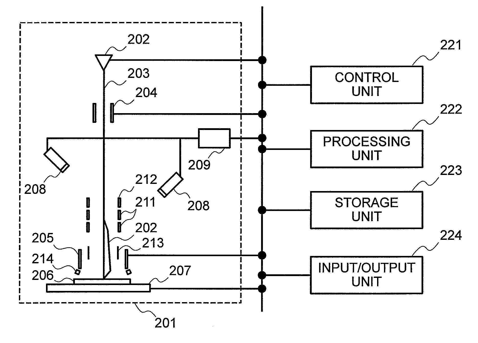
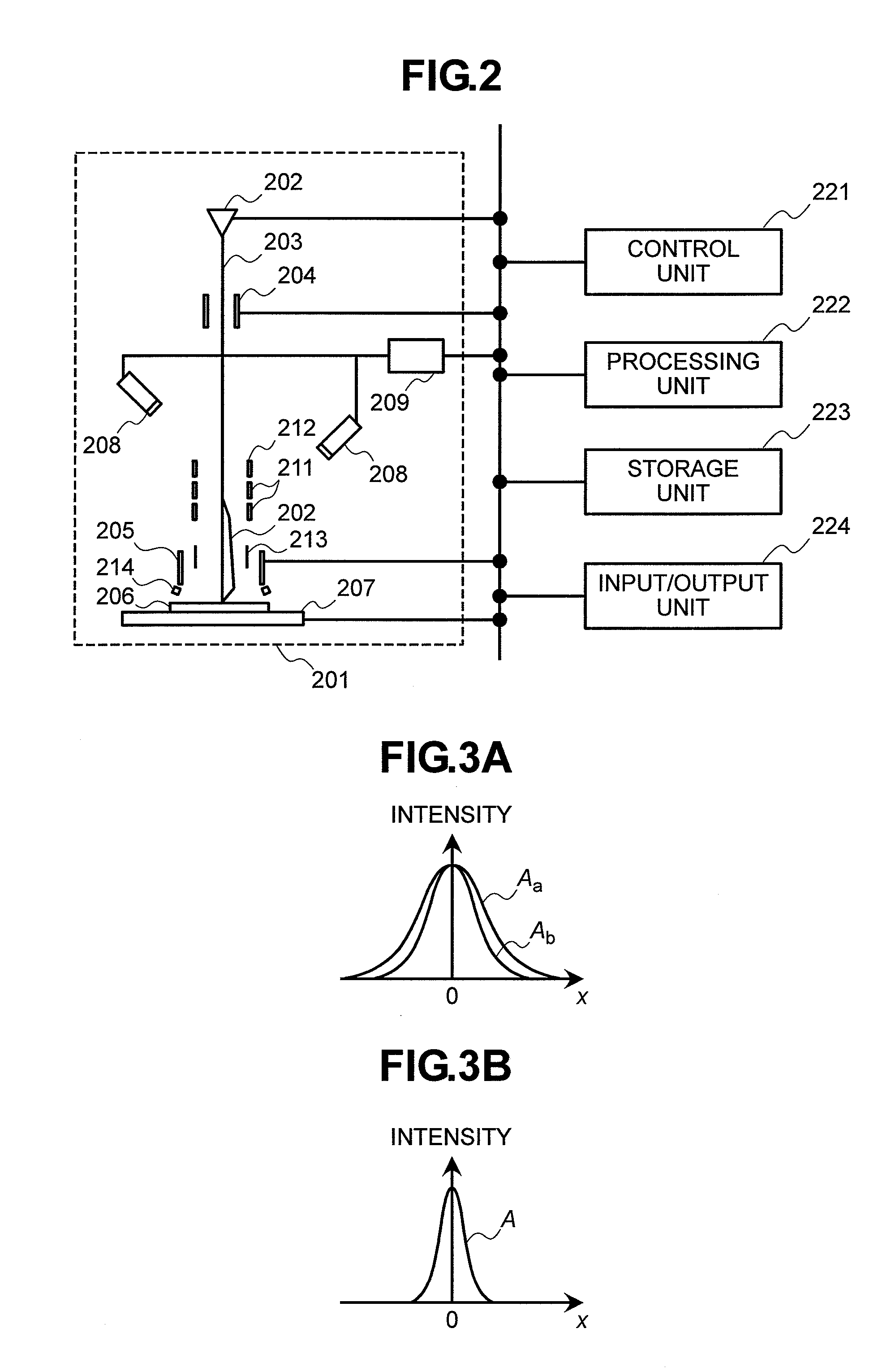
[0083]Embodiments of the case, in which the image restoration principle thus far described is applied to the defect review SEM, are described in the following.
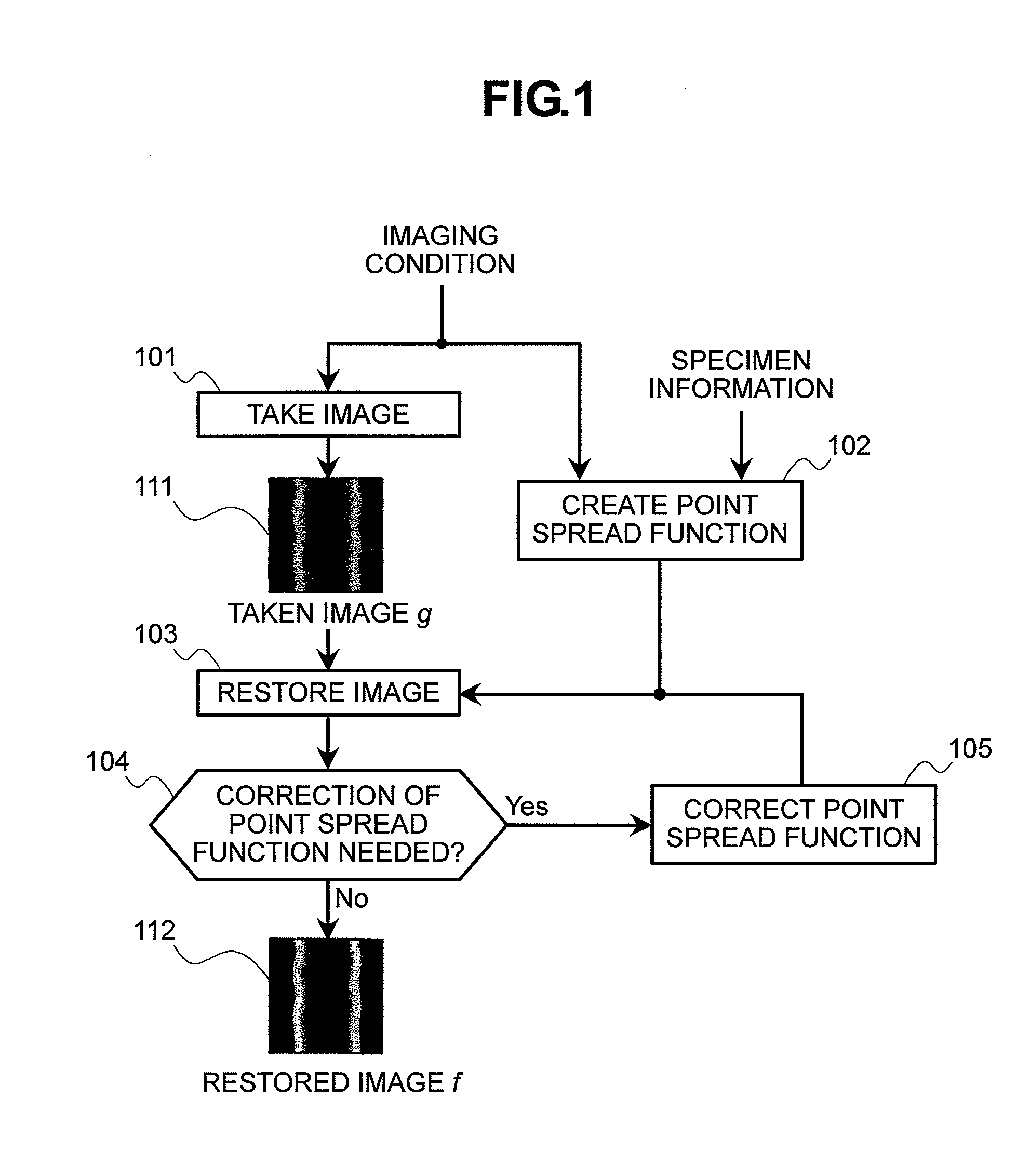
[0084]The restored image, which has been restored to a high resolving power or a high S / N ratio, can also be employed for observing a minute constitution or a high-precision measurement. FIG. 14 shows one embodiment of a sequence of performing a defect detection or a defect classification by using a restored image obtained by an image restoration in the semiconductor inspecting SEM such as the SEM inspecting device or the defect review SEM. Steps 101 to 105 are identical to those of Steps described with reference to FIG. 1. The restored image 112 is subjected to the detection of a defect or the classification into the defect kind at Step 1301. In the case where the defect detection is made on the taken image of the prior art, the taken image of a low resolving power or a low S / N ratio may be unable to be detected of its defect...
embodiment 2
[0090]Here is described an embodiment of the case, in which the aforementioned image restoration principle is applied to the semiconductor measuring SEM such as the measuring SEM.
[0091]FIG. 16 shows one embodiment of a sequence of measuring the pattern size and shape by using the restored image in the semiconductor measuring SEM such as the measuring SEM. The sequence of 101 to 105 is identical to that of FIG. 1. The restored image 112 is subjected at Step 1201 to the size measurement or shape measurement of the pattern contained in the image. This operation is performed in the measuring SEM or the like at the point (or the evaluation point), where the size measurement, the shape measurement or the like is to be performed. In the measuring SEM, the taken image is ordinarily produced by detecting the secondary electrons.
[0092]If the image is produced to have the higher luminosity coefficient for the larger number of secondary electrons, it is possible to obtain an image, which can fo...
PUM
| Property | Measurement | Unit |
|---|---|---|
| scanning electron microscope | aaaaa | aaaaa |
| image processing | aaaaa | aaaaa |
| size | aaaaa | aaaaa |
Abstract
Description
Claims
Application Information
 - R&D
- Intellectual Property
- Life Sciences
- Materials
- Tech Scout
- Unparalleled Data Quality
- Higher Quality Content
- 60% Fewer Hallucinations
Browse by: Latest US Patents, China's latest patents, Technical Efficacy Thesaurus, Application Domain, Technology Topic, Popular Technical Reports.
© 2025 PatSnap. All rights reserved.Legal|Privacy policy|Modern Slavery Act Transparency Statement|Sitemap|About US| Contact US: help@patsnap.com


