Semiconductor device

a technology of semiconductor devices and semiconductors, applied in the direction of logic circuit coupling/interface arrangements, pulse techniques, instruments, etc., can solve the problems of inability to measure the delay in the circuit of the signal delay in the output buffer is quite small compared, so as to improve the observability of the output buffer, improve the reliability, and measure the signal delay in the output buffer with accuracy

Inactive Publication Date: 2008-09-25
RENESAS ELECTRONICS CORP
View PDF2 Cites 9 Cited by
  • Summary
  • Abstract
  • Description
  • Claims
  • Application Information

AI Technical Summary

Benefits of technology

[0010]According to the semiconductor device of the present invention, it is possible to monitor signals that are transmitted in the output buffer. In other words, according to the semiconductor device of the present invention, it is possible to measure the signal delay in the output buffer with accuracy without being influenced by the parasitic capacitance of the line connected to the external output terminal.
[0011]The semiconductor device according to the present invention achieves high reliability by improving observability in the output buffer.

Problems solved by technology

In recent years, there has been a problem in a semiconductor device that signal delay is occurred in the semiconductor device along with miniaturization of a manufacturing process and this signal delay causes malfunction.
However, the signal delay occurred in the circuit of the output buffer is quite small compared with the signal delay occurred in the line capacitor.
Therefore, in the conventional example, the delay occurred in the circuit of the output buffer cannot be measured with accuracy.

Method used


Image

  • Semiconductor device
  • Semiconductor device
  • Semiconductor device

Examples


first embodiment

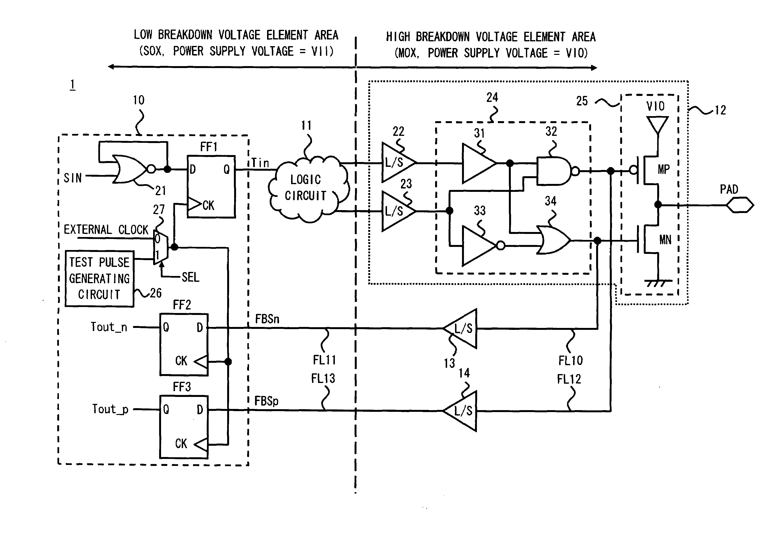
[0019]The embodiment of the present invention will be described hereinafter with reference to the drawings. FIG. 1 shows a circuit diagram of an output buffer 12 and other peripheral circuit in a semiconductor device 1 according to the first embodiment. Although FIG. 1 shows a delay test circuit 10, a logic circuit 11, and level shift circuits 13 and 14 as the peripheral circuit, the semiconductor device 1 may include other circuits that are not shown.

[0020]Power supply voltage in the delay test circuit 10 and the logic circuit 11 is internal power supply voltage VII, and power supply voltage in the output buffer 12 and the level shift circuits 13 and 14 is output power supply voltage VIO that is higher than the internal power supply voltage. The delay test circuit 10 and the logic circuit 11 are formed by low breakdown voltage element and formed in a low breakdown voltage element area of the area where the semiconductor device is formed. The output buffer 12 and the level shift cir...


PUM


Abstract

A semiconductor device according to the present invention includes an internal circuit executing a predetermined processing based on signal input from an external device, an output buffer driving line connected to an output terminal based on signal output from the internal circuit, a feedback line branched off from signal line in buffer transmitting data signal to an output stage circuit of the output buffer, and a delay test circuit connected to the feedback line.

Description

BACKGROUND OF THE INVENTION[0001]1. Field of the Invention[0002]The present invention relates to a semiconductor device, and more particularly, to a semiconductor device including a delay test circuit measuring signal delay generated in an internal circuit of the semiconductor device.[0003]2. Description of Related Art[0004]In recent years, there has been a problem in a semiconductor device that signal delay is occurred in the semiconductor device along with miniaturization of a manufacturing process and this signal delay causes malfunction. In order to measure this signal delay, a delay test circuit is often embedded in the semiconductor so as to measure the signal delay in the semiconductor device.[0005]The signal delay is also occurred in an output of the semiconductor device. The signal delay in the output is occurred by resistance component or capacitance component that is parasitic in line connected to an external output terminal. Further, in the semiconductor device that is m...

Claims


Application Information

Patent Timeline
Patent Type & Authority Applications(United States)
IPC IPC(8): H03K19/00
CPCG01R31/31716H03K19/003G01R31/31725
Inventor MIYAZAKI, YOUKONNO, MAMORU
Owner RENESAS ELECTRONICS CORP
Why Eureka
Try Eureka