Color filter substrate, manufacturing method thereof and liquid crystal display

a technology of color filter substrate and liquid crystal display, which is applied in the field of color filter substrate, can solve the problems of reducing reducing the uniformity of electrical fields, and affecting the display quality of liquid crystal display, so as to increase the luminance uniformity of lcd, reduce the and reduce the effect of non-uniformity of electrical fields

Active Publication Date: 2008-07-31
BEIJING BOE OPTOELECTRONCIS TECH CO LTD +1
View PDF1 Cites 14 Cited by
  • Summary
  • Abstract
  • Description
  • Claims
  • Application Information

AI Technical Summary

Benefits of technology

[0014]Compared with the conventional color filter substrate, since a counter electrode is formed of a double-layer structure of a transparent conductive layer / a metal conductivity-enhanced layer or a metal conductivity-enhanced layer / a transparent conductive layer in the area corresponding to the black matrix, the color filter substrate of the embodiments of the present invention can effectively reduce the sheet resistance of the counter electrode and increases the luminance uniformity of the LCD comprising the color filter substrate and the transmittance of the transparent conductive layer of the pixel area is not influenced. The color filter substrate according to the embodiments of the present invention can be used for a large size LCD, for example, a TV set. In the color filter substrate of the embodiments of the present invention, a transparent conductive layer / a metal conductivity-enhanced layer double structure or a metal conductivity-enhanced layer / a transparent conductive layer double structure may be directly formed on the substrate first. This planar electrode design can effectively reduce the non-uniformity of the electrical field generated in the central portion and at the edge of the pixel areas and increase the display quality of the LCD.

Problems solved by technology

On the other hand, for a whole LCD device, too large sheet resistance means increased power consumption.
Such step leads to unevenness of the transparent conductive film 4, further causes non-uniformity of the electrical field formed in the central portion and at the edge of the pixel areas and degrades the image quality. FIG. 2 shows the distribution|[zhan1] of the electrical field formed between the two substrates.

Method used


Image

  • Color filter substrate, manufacturing method thereof and liquid crystal display
  • Color filter substrate, manufacturing method thereof and liquid crystal display
  • Color filter substrate, manufacturing method thereof and liquid crystal display

Examples


first embodiment

The First Embodiment

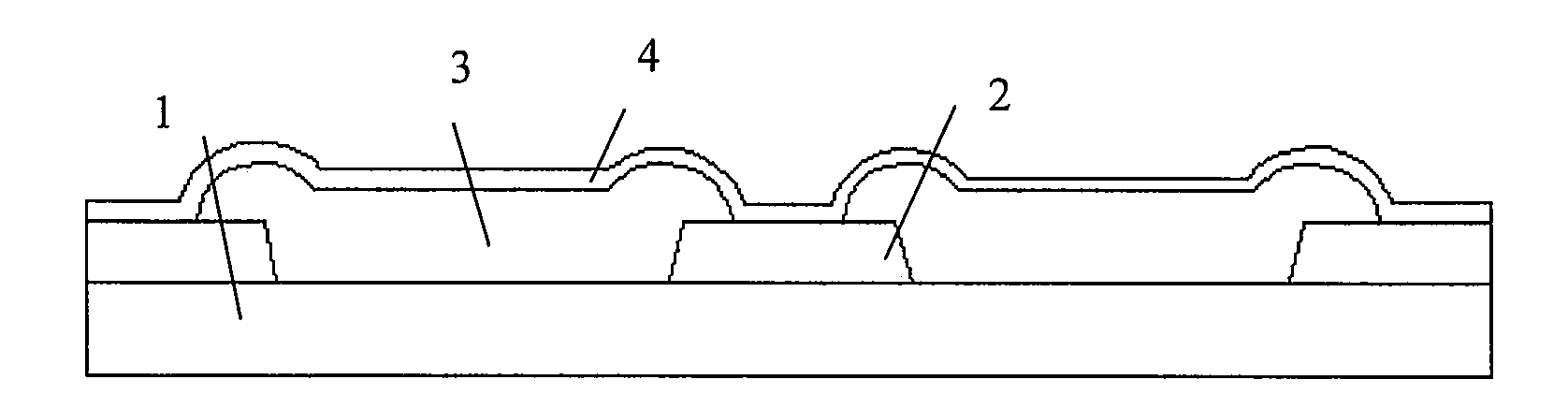
[0026]FIG. 3 is a plan view of a color filter substrate according to the first embodiment of the present invention, and FIG. 4 is a cross-sectional view of the color filter substrate taken along the line A-A in FIG. 3. As shown in FIGS. 3 and 4, the color filter substrate comprises a substrate 1 such as a glass substrate, and a black matrix 2, a color filter layer 3, a transparent conductive layer 4, and the like, which are formed on the substrate 1. The black matrix 2 is provided on the surface of the substrate 1, and the black matrix 2 has a plurality of grid areas. The substrate surface within each of the grid areas is exposed. The color filter layer 3 is provided in each of the grid areas of the black matrix 2 and partially overlaps with the black matrix 2 in order to prevent light leakage. The transparent conductive layer 4 covers the color filter layer 3 and the black matrix 2, and the transparent conductive layer 4 may be a layer of indium tin oxide (ITO),...

second embodiment

The Second Embodiment

[0028]FIG. 5 is a schematic cross-sectional view of the color filter substrate according to the second embodiment of the invention. As shown in FIG. 5, the color filter comprises a substrate 1 and a black matrix 2, a color filter layer 3, a transparent conductive layer 4, and the like, which are formed on the substrate 1. In the second embodiment, the transparent conductive layer 4 is formed directly on the substrate 1, and then a metal conductivity-enhanced layer 5, such as a layer of copper (Cu), aluminum (Al), molybdenum (Mo), zinc (Zn), silver (Ag) or an alloy thereof, is deposited in an area on the surface of the layer 4 in which the black matrix 2 is to be formed later and contacts the transparent conductive layer 4. Subsequently, the black matrix 2 is provided above the transparent conductive layer 4 and the metal conductivity-enhanced layer 5, and the black matrix 2 has a plurality of grid areas, through which the surface of the transparent conductive la...

third embodiment

The Third Embodiment

[0030]FIG. 7 is a schematic cross-sectional view of a color filter substrate according to the third embodiment of the invention. As shown in FIG. 7, the color filter substrate in the third embodiment is similar to that in the second embodiment, except that a metal conductivity-enhanced layer 5 is first formed in an area on a substrate 1 corresponding to a black matrix 2 to be formed. Subsequently, a transparent conductive layer 4 is formed on the metal conductivity-enhanced layer 5, and then the black matrix 2 and a color filter layer 3 are formed on the transparent conductive layer 4. The black matrix 2 has a plurality of grid areas, and the surface of the transparent conductive layer 4 within each of the grid areas is exposed. The color filter layer 3 is provided in each of the grid areas of the black matrix 2 and partially overlaps with the black matrix 2 in order to prevent light leakage.

[0031]Also, in the third embodiment, a double-layer structure of the met...


PUM


Abstract

Provided is a color filter substrate that comprises a substrate. A black matrix, a color filter layer, and a transparent conductive layer are formed on the substrate and the color filter layer is formed in a pixel area defined by the black matrix. A metal conductivity-enhanced layer is formed above and / or below the transparent conductive layer and contacts with the transparent conductive layer in an area corresponding to the black matrix.

Description

[0001]The present application claims the priority of Chinese patent application No. 200710063049.1 filed on Jan. 25, 2007 with the Chinese Intellectual Property Office, which is incorporated herewith by reference.BACKGROUND OF THE INVENTION[0002]The present invention relates to a color filter substrate, a method for manufacturing the same, and a liquid crystal display (LCD).[0003]With development of the display technologies, thin film transistor liquid crystal displays (TFT LCDs) have become the mainstream of the display market. Currently, a TFT LCD is developed to have the characteristics of full color, large size, high definition, etc. Color filters are important for a TFT LCD device to realize colorful display. A TFT LCD generally comprises a TFT array substrate, a color filter substrate, and a liquid crystal layer interposed therebetween.[0004]Generally, the color filter substrate is constructed so that a black matrix (BM) is provided on a transparent glass substrate for shieldi...

Claims


Application Information

Patent Timeline
IPC IPC(8): G03F1/00
CPCG02F1/1343G02F2201/121G02F1/13439
Inventor ZHAN, HONGMING
Owner BEIJING BOE OPTOELECTRONCIS TECH CO LTD
Why Eureka
Try Eureka