


Quick Research
Generate reliable direction feasibility study reports for your R&D in just a few steps.

Technical Q&A
Discover and master advanced knowledge NOW. Basics, ideas, possibilities, all at once.

Find Solutions
As an expert in R&D theories, this can generate solutions to your technical problems instantly.

Evaluate Feasibility
Analyze your overall solution with one click, know your potential R&D risks in advance.

Monitor Landscape
Get weekly tech updates, stay abreast of the latest tech innovations and key insights.
Combined Solderable Multi-Purpose Surface Finishes on Circuit Boards and Method of Manufacture of Such Boards
a technology of surface finishes and circuit boards, applied in the field of pwb, can solve the problems of still suffering from the same problems, and achieve the effect of fast pores
- Summary
- Abstract
- Description
- Claims
- Application Information
AI Technical Summary
Benefits of technology
Problems solved by technology
Method used
Image


Examples
Embodiment Construction
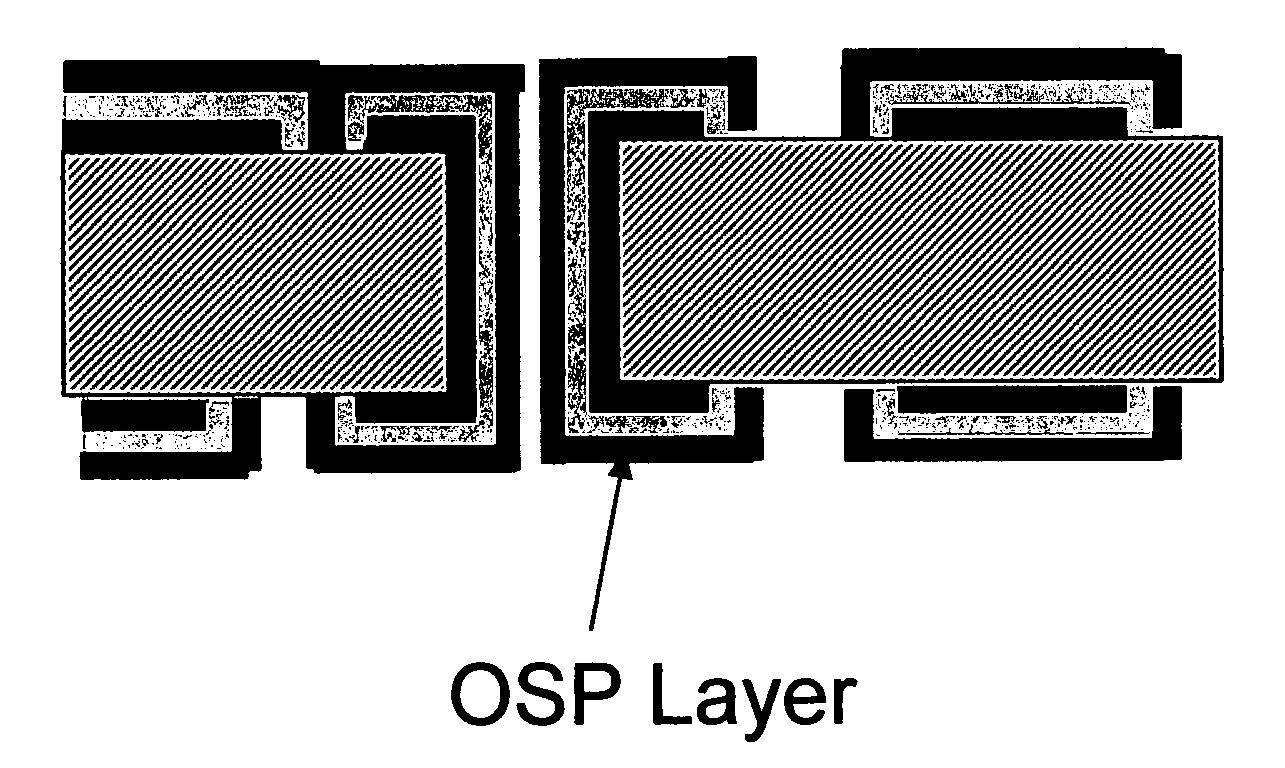
[0004]FIG. 1 illustrates a PWB having a substrate, normally a material, such as glass reinforced epoxy, on which numerous layers may be formed. While the substrate illustrated in this embodiment is composed of glass reinforced epoxy, those skilled in the art will realize that the substrate may be composed of any substrate materials, including epoxies, polyimides, fluorinated polymers, ceramics, polyesters, phenolics, and aramide paper. A base copper laminate or similar laminate material is place over the entire substrate. Following the application of the base copper laminate, a photo resist layer is then applied on top of the base copper laminate. The photo resist layer is then exposed to ultraviolet light which exposes the circuit trace pattern thereon and the circuit trace pattern is formed as seen in FIG. 1. Using an acid copper plating method, an electrolytic copper plate is formed in the opening created by the photo resist, and on top of the base copper laminate. However, other...
PUM
 Abstract
Description
Claims
Application Information
 - R&D Engineer
- R&D Manager
- IP Professional
- Industry Leading Data Capabilities
- Powerful AI technology
- Patent DNA Extraction
Browse by: Latest US Patents, China's latest patents, Technical Efficacy Thesaurus, Application Domain, Technology Topic, Popular Technical Reports.
© 2024 PatSnap. All rights reserved.Legal|Privacy policy|Modern Slavery Act Transparency Statement|Sitemap|About US| Contact US: help@patsnap.com