Methods for plasma diagnostics and the measurement of thin films

a thin film and plasma technology, applied in the field of semiconductor fabrication, can solve the problems of increasing the difficulty of interlayer dielectric (ild) stages, requiring a tremendous amount of processing power for complete collection, and requiring a large amount of data, etc., to achieve the effect of enhancing the capabilities of processing and measurement equipment, and reducing the integration time associated

Inactive Publication Date: 2008-07-03
LAM RES CORP
View PDF1 Cites 10 Cited by
  • Summary
  • Abstract
  • Description
  • Claims
  • Application Information

AI Technical Summary

Benefits of technology

[0021]The advantages of the present invention are numerous. Facilitation of film measurement and in-situ plasma diagnostics through the use of parallel analysis and processing provides an efficient alternative to traditional means of acquiring process information. The present method improves the use of the above discussed technology by providing a technique for reducing the integration time associated with the obtaining and processing of signals from an illumination source off a wafer surface or from plasma emissions. By splitting the incoming optical signal to different arrays and processors, integration of one data point or sample is not necessarily limited by traditional backlogs in acquisition and processing time of the previous inspection point or data sample. Faster sample rates and efficient processing enhance the capabilities of processing and measurement equipment. It is to be understood that the foregoing general description and the following detailed description are exemplary and explanatory only and are not restrictive of the invention, as claimed.

Problems solved by technology

Properties of materials on the substrate are carefully monitored throughout the fabrication process, but the task is more difficult during interlayer dielectric (ILD) stages, that is, when stacks consist of multiple dielectric and metal film layers.
Measurement systems utilizing spectral information, especially those that provide full surface mapping require a tremendous amount of processing power for complete collection, storage and analyzing of data retrieved by the sensors.
The problem with known approaches is that the amount of data is necessarily limited by the speed of the associated computer or processor.

Method used


Image

  • Methods for plasma diagnostics and the measurement of thin films
  • Methods for plasma diagnostics and the measurement of thin films
  • Methods for plasma diagnostics and the measurement of thin films

Examples


Embodiment Construction

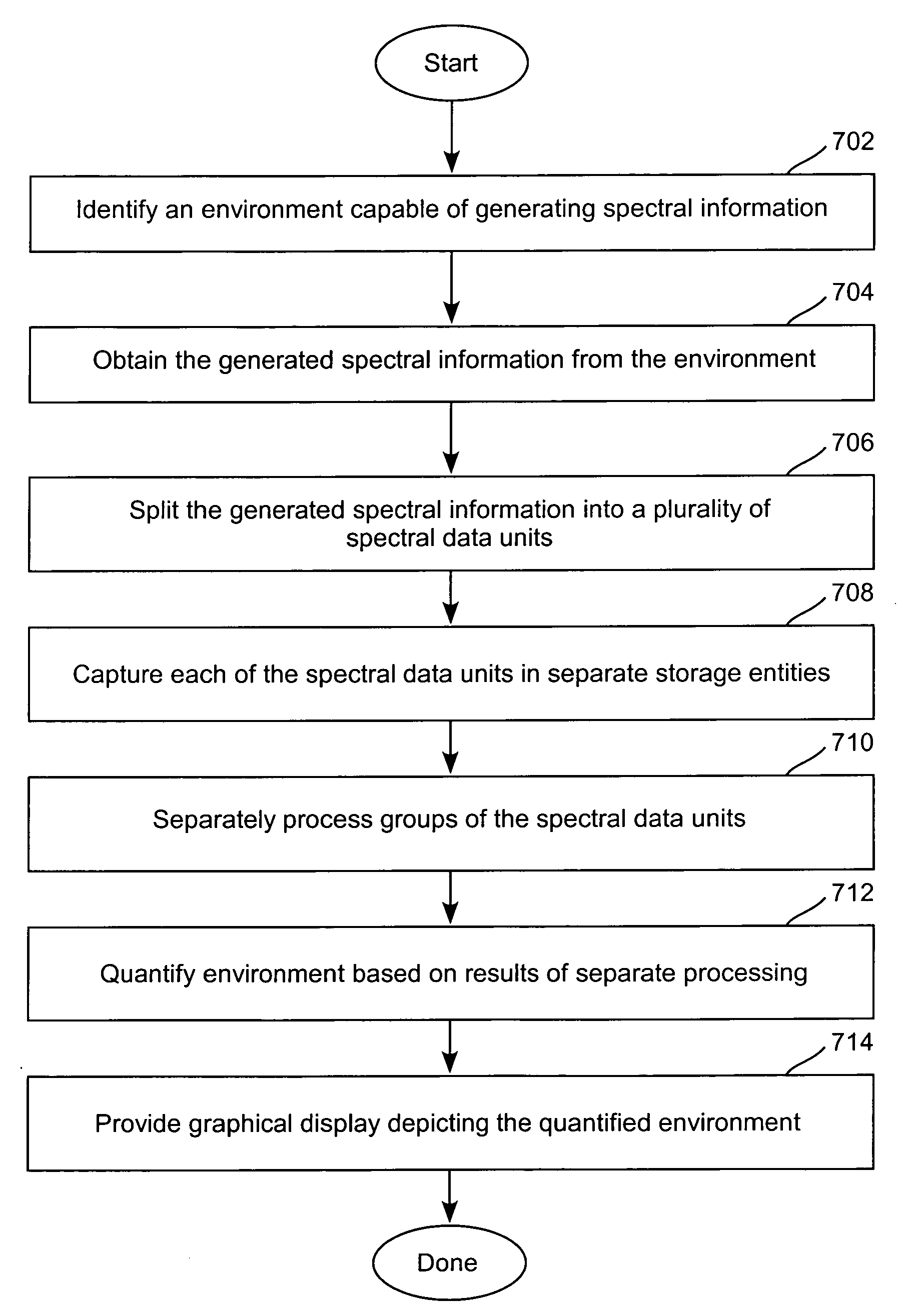
[0036]This disclosure describes a method and apparatus for reducing processing times in plasma diagnostic tools and thin-film measurement tools. Several exemplary embodiments of the invention will now be described in detail with reference to the accompanying drawings. In the following description, numerous specific details are set forth in order to provide a thorough understanding of the present invention. It will be understood, however, to one skilled in the art, that the present invention may be practiced without some or all of these specific details. In other instances, well known process operations have not been described in detail in order not to unnecessarily obscure the present invention.

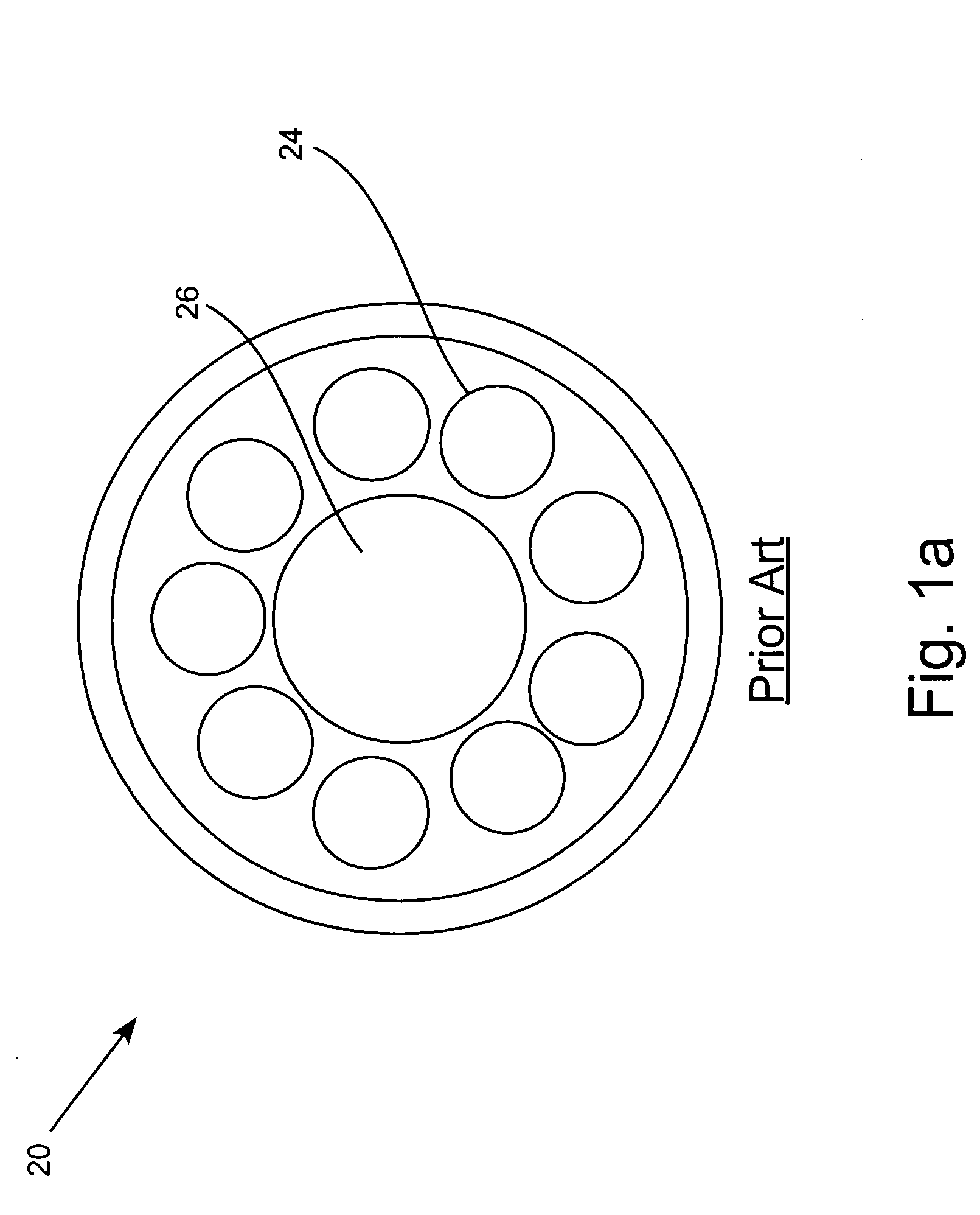
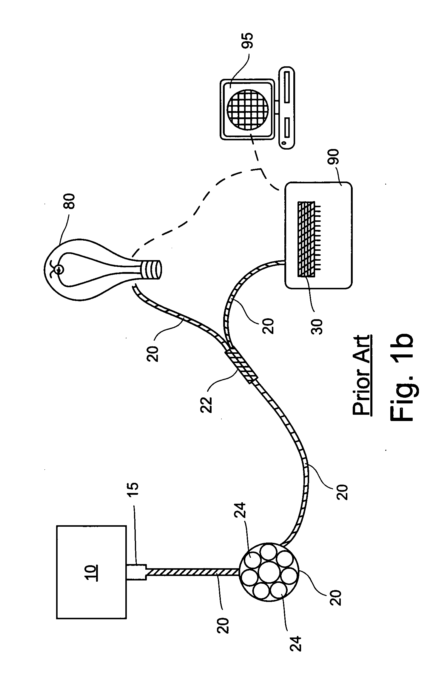
[0037]A typical spectral collection and analysis tool is shown in FIG. 1b. A fiberoptic cable 20, or other transmission medium, is coupled to an environment such as a chamber 10 by a collimator 15, and is capable of collecting light returning from a surface of a wafer being processed, or alte...


PUM


Abstract

Methods for obtaining and analyzing data from a spectral source is provided. The method includes identifying an environment that is capable of generating spectral information, and obtaining the generated spectral information from the environment. The method further includes splitting the generated spectral information into a plurality of spectral data units. The spectral data units are further captured in separate storage entities and separately processed in parallel in order to produce a complete processing and quantification of the environment.

Description

CLAIM OF PRIORITY[0001]This application is a divisional application of U.S. application Ser. No. 11 / 016,155, filed on Dec. 17, 2004, and entitled “Method and Apparatus for Plasma Diagnostics and the Measurement of Thin Films”, which is herein incorporated by reference.CROSS REFERENCE TO RELATED APPLICATIONS[0002]This application is related to U.S. patent application Ser. No. 10 / 810,209, entitled “METHOD AND APPARATUS FOR MEASUREMENT OF THIN FILMS AND RESIDUES ON SEMICONDUCTOR SUBSTRATES,” filed on Mar. 26, 2003. The disclosure of this patent application is incorporated herein by reference.BACKGROUND OF THE INVENTION[0003]1. Field of the Invention[0004]The invention relates generally to semiconductor fabrication and more specifically to measurement of films and plasma emissions during wafer processing.[0005]2. Description of the Related Art[0006]In the fabrication of semiconductor devices, there is a need to measure material features on substrates. Typically, integrated circuit devic...

Claims


Application Information

Patent Timeline
IPC IPC(8): G01J3/00
CPCG01B11/0625G01J3/443G01N2021/8411G01N21/73G01N21/8422G01N21/211
Inventor CRAVEN, DAVIDROBERTS, RYAN
Owner LAM RES CORP
Why Eureka
Try Eureka