
Semiconductor Device and Method of Forming the Same

a semiconductor and device technology, applied in the direction of semiconductor devices, basic electric elements, electrical appliances, etc., can solve the problems of reducing the capacitance across the insulating layer, inefficient device power consumption, and reducing the performance of any mosfet device comprising this structur

Inactive Publication Date: 2008-06-12
FREESCALE SEMICON INC
View PDF3 Cites 10 Cited by
  • Summary
  • Abstract
  • Description
  • Claims
  • Application Information

AI Technical Summary

Benefits of technology

"The present invention provides a semiconductor device and method of forming a semiconductor device that includes a barrier layer that allows for the continued performance of a high temperature oxygen ambient anneal without compromising the dielectric EOT or the metal gate electrode. The barrier layer is deposited at low temperatures and is resistant to ambients present in process steps subsequent to the deposition of the barrier layer and is easily etchable when needed. The deposition of the barrier layer is also compatible with existing processing techniques."

Problems solved by technology

However, the gate insulator layer and the gate electrode layers do not always share the same profile.
However, forming thinner layers of silicon dioxide as the gate insulator layer leads to leakage, i.e. current flowing through the gate dielectric resulting in inefficient device power consumption.
However, when the high-K dielectric layer is employed, it is difficult to carry out the reoxidation step, because high-K films are not good oxygen barriers, resulting in the silicon dioxide sub-layer, known as the interfacial layer, increasing in width, thereby degrading the so-called Equivalent Oxide Thickness (EOT) and hence reducing the capacitance across the insulating layer.
Clearly, this decreases the performance of any MOSFET device comprising this structure.
Performing a conventional reoxidation step on a metal gate electrode may result in oxidisation of the metal, thereby compromising the integrity of the gate electrode.
Thus, the reoxidation step cannot be performed with metal gate electrodes.

Method used


Image

  • Semiconductor Device and Method of Forming the Same
  • Semiconductor Device and Method of Forming the Same
  • Semiconductor Device and Method of Forming the Same

Examples


Embodiment Construction

[0024]Throughout the following description identical reference numerals will be used to identify like parts.

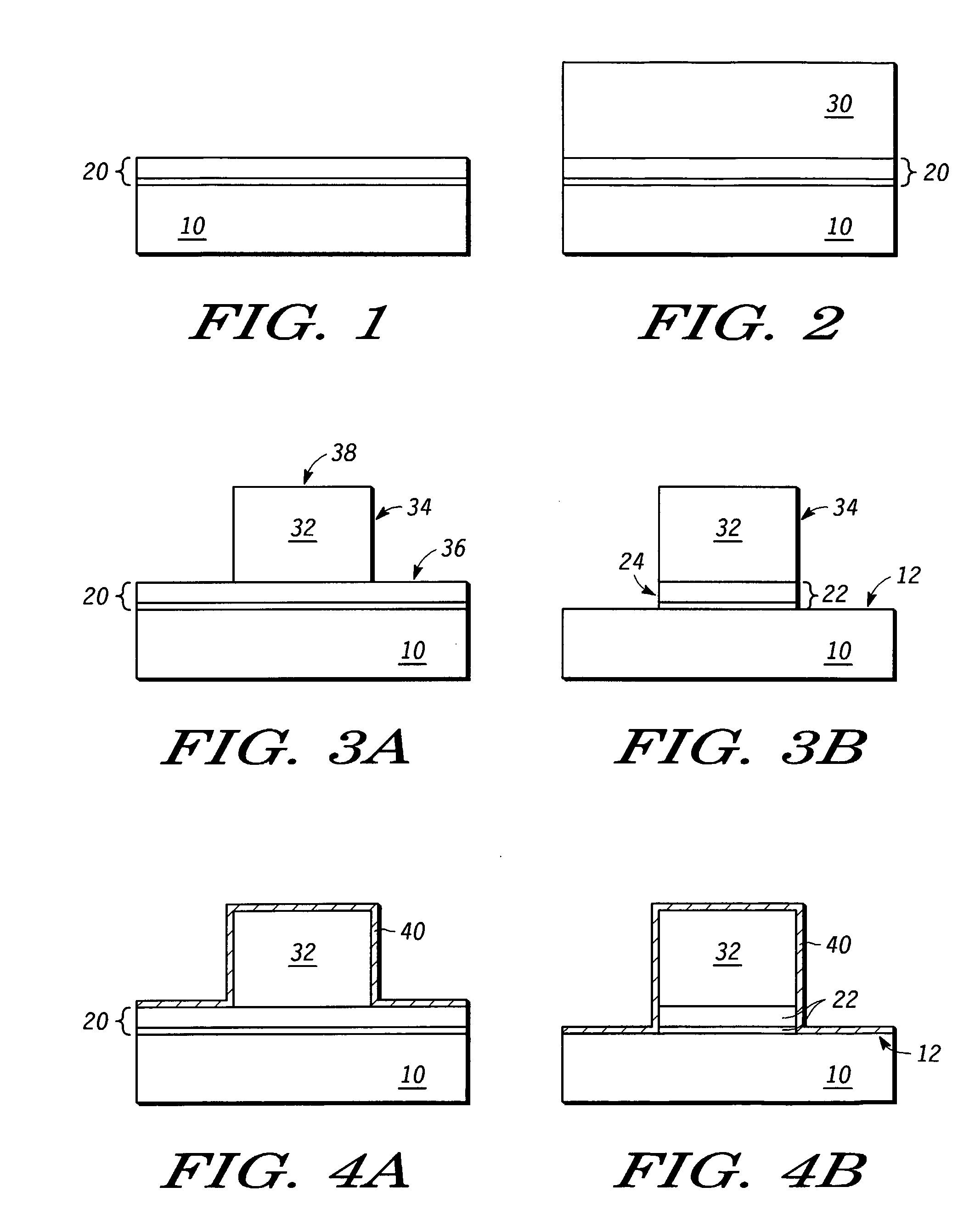
[0025]Referring to FIG. 1, a silicon substrate 10 is grown in accordance with a known Complementary Metal Oxide Semiconductor (CMOS) processing technique. Alternatively, the substrate could be a the Silicon On Insulator (SOI) substrate.

[0026]Using a known suitable deposition technique, a dielectric material, for example silicon dioxide (SiO2), or typically a material with a dielectric constant greater than that of silicon, known as a high-K material, is then deposited as a gate insulator layer 20, on the substrate 10. The gate insulator layer 20 is grown to a thickness sufficient to constitute a high quality dielectric layer. Typically, the gate insulator layer 20 is grown to a thickness of between about 15 and 30 Angstroms depending on the dielectric constant of the material and the technological application.

[0027]However, it should be appreciated that the initial thickness o...


PUM


Abstract

It is known to provide a reoxidation step in the manufacture of a MOSFET that serves a number of structural purposes in relation to the MOSFET. However, the need to provide materials of high dielectric constant for gate insulator layers of MOSFETs to accommodate a drive for smaller integrated circuits has led to excessive growth of an SiO2 interfacial layer between the gate insulator layer and a substrate. Excessive growth of the SiO2 layer results in an Effective Oxide Thickness that leads to increased leakage current in the MOSFET. Further, the replacement of polysilicon with metals as electrodes precludes oxygen exposure during processing. Consequently, the present invention provides replacing or preceding the reoxidation step with the deposition of an oxygen barrier layer over at least side walls of a gate electrode of the MOSFET, thereby providing a barrier for oxygen diffusion to the dielectric interface and metal gate electrode that prevents EOT increase and preserves metal gate electrode integrity.

Description

FIELD OF THE INVENTION[0001]The present invention relates to a method of forming a semiconductor device of the type, for example, comprising a barrier layer over at least side walls of a gate electrode, such as a Field Effect Transistor. The present invention also relates to a method of forming a semiconductor device of the type, for example, requiring the formation of a barrier layer, such as a Field Effect Transistor.BACKGROUND OF THE INVENTION[0002]In the field of semiconductor devices, it is well known to form Metal Oxide Semiconductor Field Effect Transistors (MOSFETs) having a gate, source and drain. Typically, the gate is formed by depositing a layer of silicon dioxide (SiO2), constituting a gate insulator layer, upon a silicon substrate and then depositing a polysilicon layer, constituting a gate electrode layer, upon the gate insulator layer. The gate electrode layer, and optionally the gate insulator layer is then etched to form an appropriately shaped gate. However, the g...

Claims


Application Information

Patent Timeline
Patent Type & Authority Applications(United States)
IPC IPC(8): H01L21/336H01L29/78
CPCH01L21/28194H01L29/513H01L29/7833H01L29/6656H01L29/517
Inventor KAUSHIK, VIDYA
Owner FREESCALE SEMICON INC
Learn More