Method of Manufacturing Flash Memory Device
- Summary
- Abstract
- Description
- Claims
- Application Information
AI Technical Summary
Benefits of technology
Problems solved by technology
Method used
Image

Examples
Embodiment Construction
[0010]A specific embodiment according to the invention is described below with reference to the accompanying drawings.
[0011]FIGS. 1 to 5 are views illustrating a method of manufacturing a flash memory device according to an embodiment of the invention.
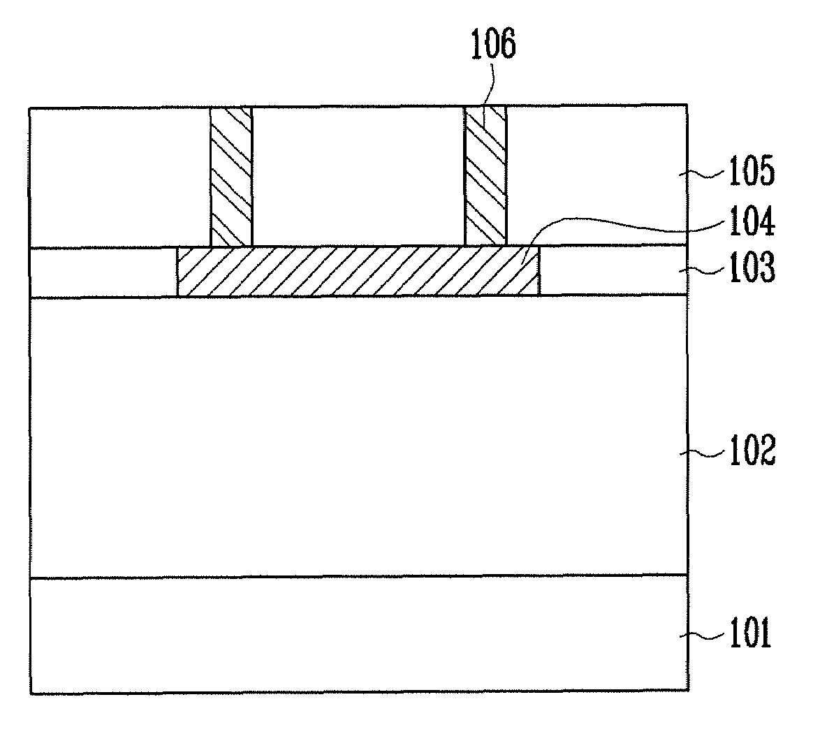
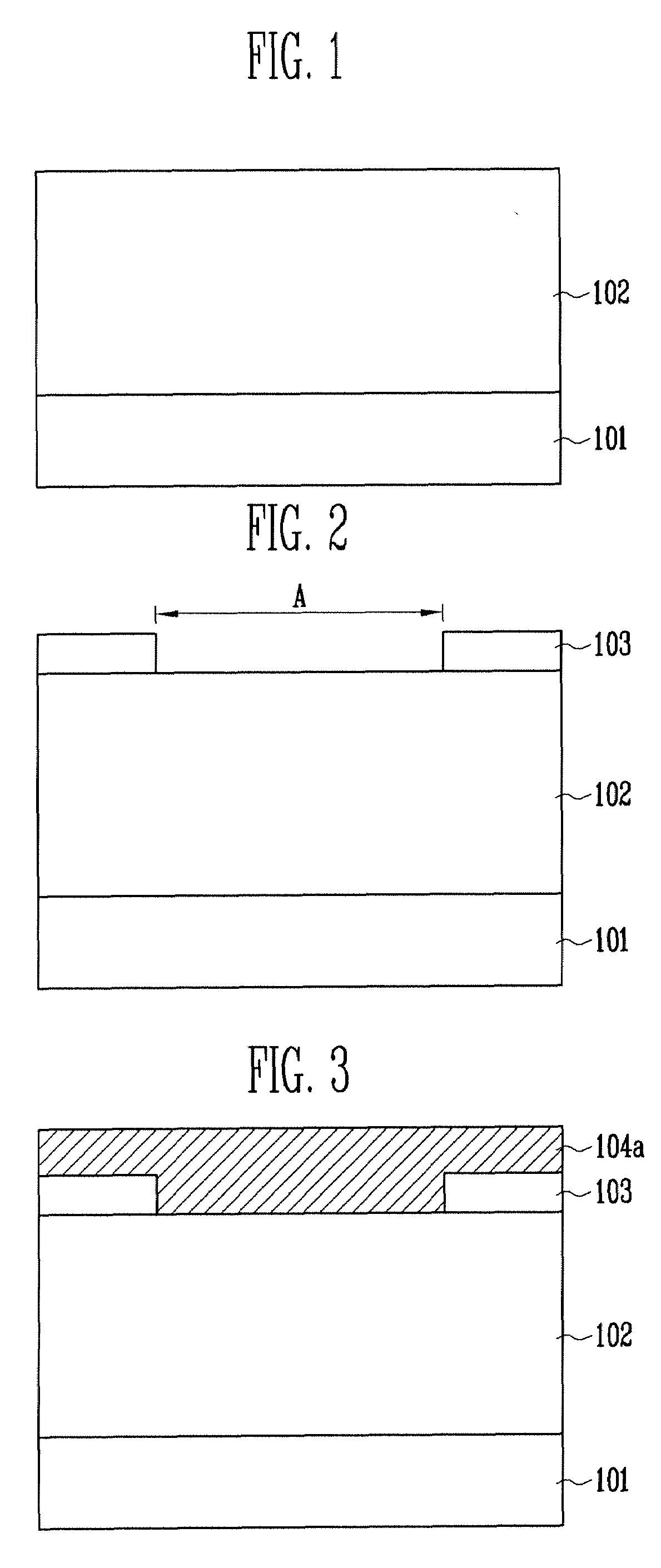
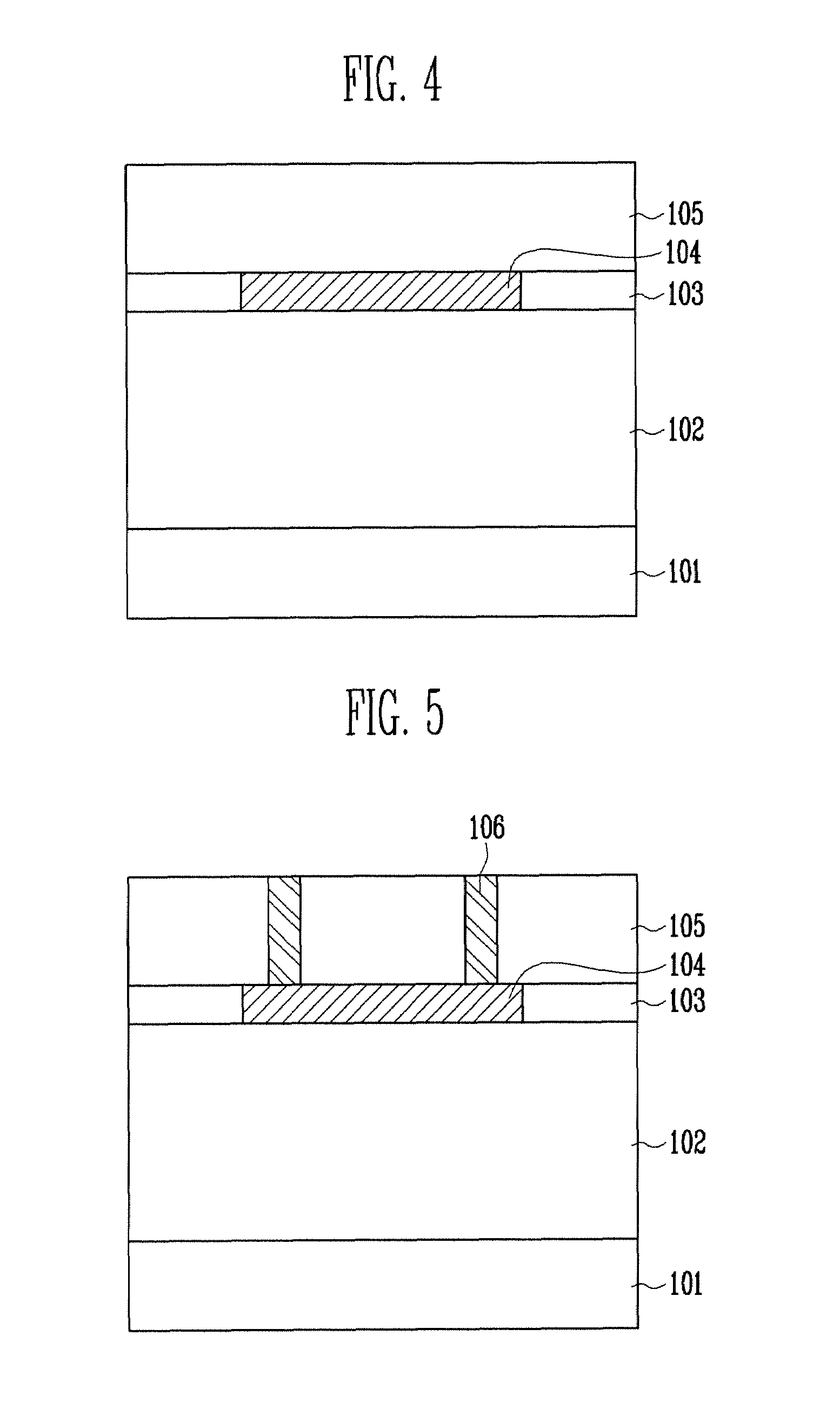
[0012]FIG. 1 illustrates a peripheral region in which a poly resistor is formed, of a cell region and the peripheral region. Steps before the poly resistor is formed are briefly described below. A first insulating layer 102 is formed over a semiconductor substrate 101 in which a gate (not illustrated) is formed. A source contact plug (not illustrated) is formed in the first insulating layer 102.
[0013]Referring to FIG. 2, a second insulating layer 103 is formed over the first insulating layer 102 including the source contact plug. A mask pattern (not illustrated) for forming a drain contact hole is formed on the second insulating layer 103. The drain contact hole (not illustrated) is formed in the first and the second insulating layers ...
PUM
 Abstract
Description
Claims
Application Information
 - R&D
- Intellectual Property
- Life Sciences
- Materials
- Tech Scout
- Unparalleled Data Quality
- Higher Quality Content
- 60% Fewer Hallucinations
Browse by: Latest US Patents, China's latest patents, Technical Efficacy Thesaurus, Application Domain, Technology Topic, Popular Technical Reports.
© 2025 PatSnap. All rights reserved.Legal|Privacy policy|Modern Slavery Act Transparency Statement|Sitemap|About US| Contact US: help@patsnap.com