
Method of fabricating a semiconductor device

a semiconductor and device technology, applied in the field of integrated circuits, can solve problems such as unsatisfactory sheet resistance, and achieve the effect of reducing the width of the spacer and improving the mobility of electrons or holes

Active Publication Date: 2008-03-27
UNITED MICROELECTRONICS CORP
View PDF1 Cites 6 Cited by
  • Summary
  • Abstract
  • Description
  • Claims
  • Application Information

AI Technical Summary

Benefits of technology

[0008]The present invention is to provide a semiconductor device and a method of fabricating the same, which improve the mobility of electrons or holes in the channel and prevent the metal silicide layers from being damaged during the subsequent etching process of reducing the width of the spacer.
[0019]In the present invention, a surface treatment step is performed before the step of reducing the width of the spacer to form a protection layer on the metal silicide layers via surface reaction, thus preventing the metal silicide layers from being damaged during the subsequent etching process of reducing the width of the spacer.

Problems solved by technology

However, when the etching process is performed, the metal silicide layers 22 and 24 are directly exposed to the etching environment without any protection, the metal silicide layers 22 and 24 will be damaged after the etching process, especially after the over etching, resulting in unsatisfactory sheet resistance.

Method used


Image

  • Method of fabricating a semiconductor device
  • Method of fabricating a semiconductor device
  • Method of fabricating a semiconductor device

Examples


Embodiment Construction

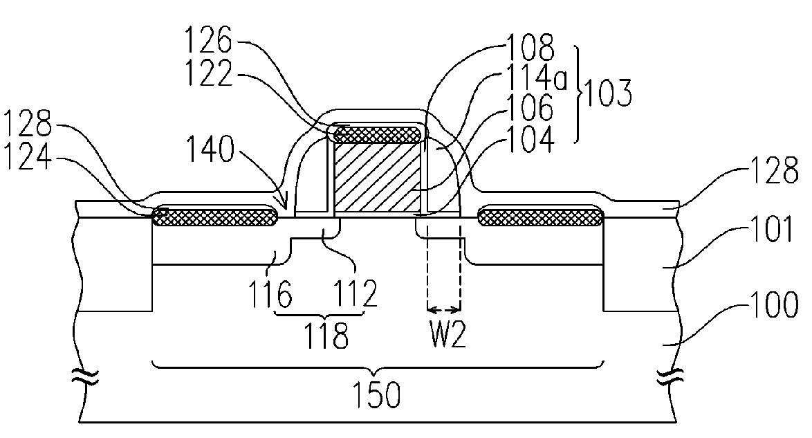
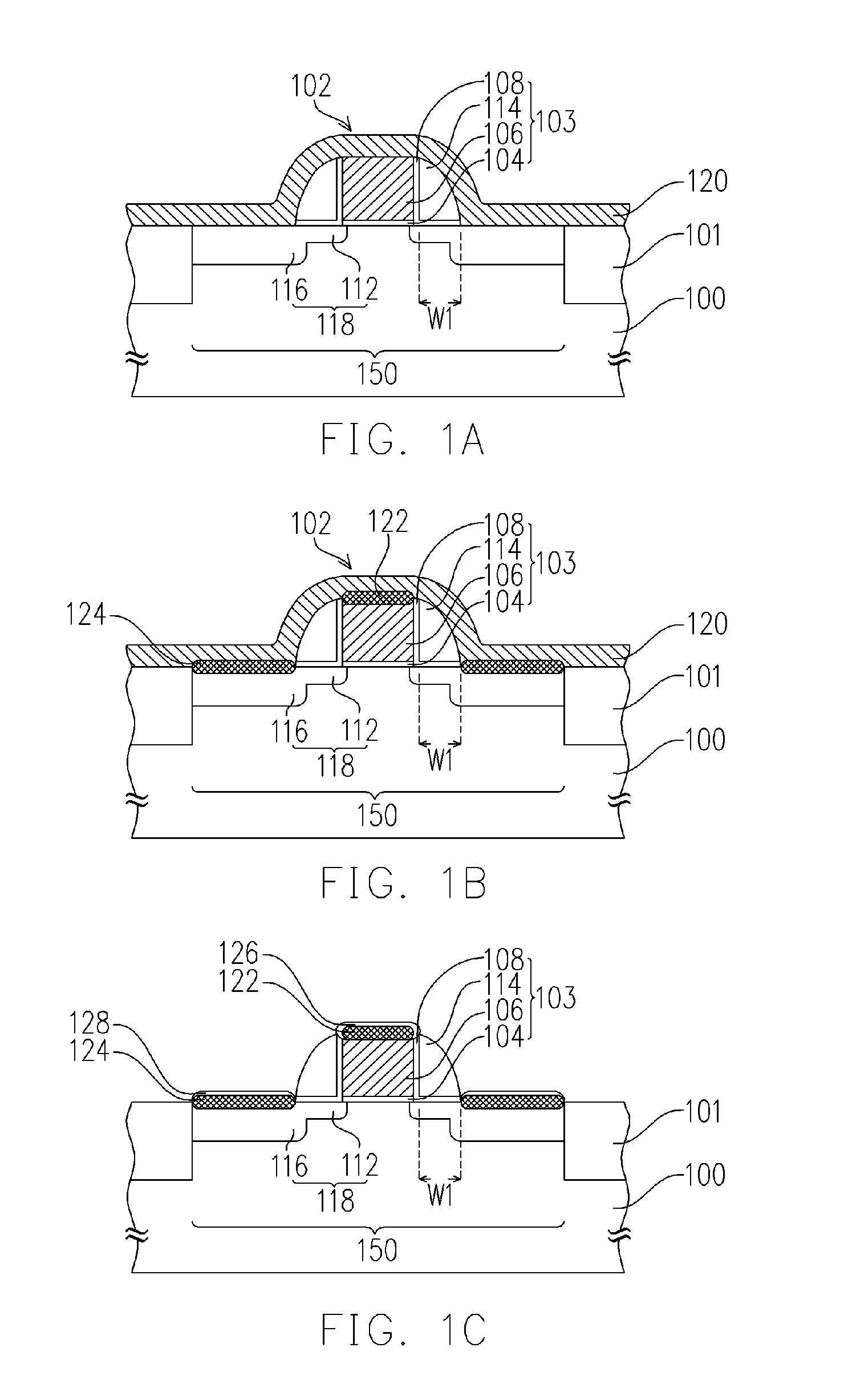
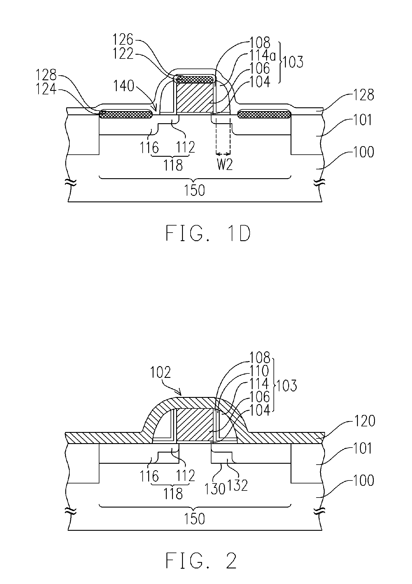
[0027]FIGS. 1A˜1D are sectional flow charts of a method of fabricating a semiconductor device according to an embodiment of the present invention.

[0028]Referring to FIG. 1A, an isolation structure 101 is formed in a substrate 100 to define an active area 150. Then, a transistor 102 is formed in the active area 150. The transistor 102 includes a gate structure 103 and a source / drain region 118.

[0029]The substrate 100 is, for example, a substrate of bulk semiconductor, or a silicon-on-insulator (SOI) substrate, such as a substrate containing silicon, epitaxial silicon, germanium, silicon germanium silicon carbide, or the combinations thereof.

[0030]The method of forming the transistor 102 is, for example, first forming a patterned gate dielectric layer 104 and a gate conductor layer 106 on the substrate 100. The gate dielectric layer 104 is, for example, a silicon oxide layer, silicon oxynitride layer, silicon nitride layer or high dielectric constant material layer with a dielectric c...


PUM

PropertyMeasurementUnit
temperatureaaaaaaaaaa
widthaaaaaaaaaa
stressaaaaaaaaaa

Abstract

A method of fabricating semiconductor device is provided. A transistor is formed on a substrate, and a metal suicide layer is formed on the surface of a gate conductor layer and a source / drain region. Next, a surface treatment process is performed to selectively form a protection layer on the surface of the metal silicide layer. Then, a spacer of the transistor is partially removed using the protection layer as a mask, so as to reduce the width of the spacer. Then, a stress layer is formed on the substrate.

Description

BACKGROUND OF THE INVENTION[0001]1. Field of Invention[0002]The present invention relates to an integrated circuit and a method of fabricating the same. More particularly, the present invention relates to a semiconductor device and a method of fabricating the same.[0003]2. Description of Related Art[0004]In common semiconductor processes, after a metal oxide semiconductor (MOS) transistor is fabricated, a stress layer will be formed on the substrate to increase the mobility of electrons or holes in the channel of the MOS transistor. In semiconductor processes with a line width lower than 65 nm, for a p-type MOS transistor, a stress layer having compressive stress can be formed on the substrate, so as to generate the compressive stress along the channel direction in the p-type MOS transistor; and for an n-type MOS transistor, a stress layer having tensile stress can be formed on the substrate, so as to generate the tensile stress along the channel direction of the n-type transistor. ...

Claims


Application Information

Patent Timeline
Patent Type & Authority Applications(United States)
IPC IPC(8): H01L21/8234
CPCH01L21/823807H01L21/823864H01L29/665H01L29/7843H01L29/6659H01L29/7833H01L29/6656
Inventor HSIEH, CHAO-CHINGCHANG, CHUN-CHIEHHUNG, TZUNG-YU
Owner UNITED MICROELECTRONICS CORP
Learn More