


Quick Research
Generate reliable direction feasibility study reports for your R&D in just a few steps.

Technical Q&A
Discover and master advanced knowledge NOW. Basics, ideas, possibilities, all at once.

Find Solutions
As an expert in R&D theories, this can generate solutions to your technical problems instantly.

Evaluate Feasibility
Analyze your overall solution with one click, know your potential R&D risks in advance.

Monitor Landscape
Get weekly tech updates, stay abreast of the latest tech innovations and key insights.
Electron beam enhanced surface wave plasma source
lectron beam technology, applied in the direction of electrolysis components, vacuum evaporation coatings, coatings, etc., can solve the problems of several deficiencies in the practical implementation of swp sources, and achieve the effect of enhancing the robustness of a surface wave plasma sour
- Summary
- Abstract
- Description
- Claims
- Application Information
AI Technical Summary
Benefits of technology
Problems solved by technology
Method used
Image


Examples
Embodiment Construction
[0029]In the following description, to facilitate a thorough understanding of the invention and for purposes of explanation and not limitation, specific details are set forth, such as a particular geometry of the plasma processing system and various descriptions of the system components. However, it should be understood that the invention may be practiced with other embodiments that depart from these specific details.
[0030]Nonetheless, it should be appreciated that, contained within the description are features which, notwithstanding the inventive nature of the general concepts being explained, are also of an inventive nature.
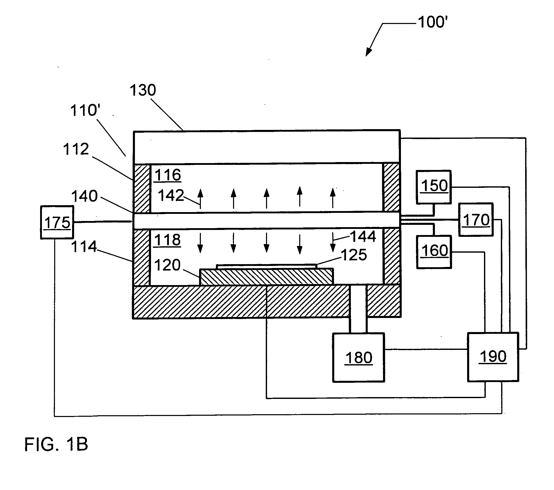
[0031]Referring now to the drawings, wherein like reference numerals designate identical or corresponding parts throughout the several views, FIG. 1A illustrates a plasma processing system 100 according to an embodiment. The plasma processing system 100 may comprise a dry plasma etching system or a plasma enhanced deposition system.
[0032]The plasma processing s...
PUM
| Property | Measurement | Unit |
|---|---|---|
| voltage | aaaaa | aaaaa |
| voltage | aaaaa | aaaaa |
| DC voltage | aaaaa | aaaaa |
Abstract
Description
Claims
Application Information
 - R&D Engineer
- R&D Manager
- IP Professional
- Industry Leading Data Capabilities
- Powerful AI technology
- Patent DNA Extraction
Browse by: Latest US Patents, China's latest patents, Technical Efficacy Thesaurus, Application Domain, Technology Topic, Popular Technical Reports.
© 2024 PatSnap. All rights reserved.Legal|Privacy policy|Modern Slavery Act Transparency Statement|Sitemap|About US| Contact US: help@patsnap.com