Thin film transistor array panel for a display device and a method of manufacturing the same

a technology of thin film transistors and array panels, which is applied in the direction of semiconductor devices, instruments, electrical apparatus, etc., can solve the problems of achieve the effects of excellent reliability and charge mobility, relatively simple manufacturing process, and low reliability and charge mobility

Inactive Publication Date: 2008-02-21
SAMSUNG ELECTRONICS CO LTD
View PDF6 Cites 27 Cited by
  • Summary
  • Abstract
  • Description
  • Claims
  • Application Information

AI Technical Summary

Benefits of technology

[0009]Such thin film transistors are classified into a bottom gate type and a top gate type according to the structures. The bottom gate type is further classified into an etch back type and an etch stopper type. The bottom gate type is mainly applied to a thin film transistor using a semiconductor formed of amorphous silicon. For the etch back type of thin film transistor, the manufacturing process is relatively simple compared with the etch stopper type, but reliability and charge mobility are low. Meanwhile, the etch stopper type has excellent reliability and charge mobility compared with the etch back type. However, in the etch stopper type, an additional manufacturing process is required to form an etch stopper.
[0010]Embodiments of the present invention have been made in an effort to provide a thin film transistor array panel for a display device and a method of manufacturing the same, having advantages of simplifying a manufacturing process of an etch stopper type of thin film transistor array panel.

Problems solved by technology

For the etch back type of thin film transistor, the manufacturing process is relatively simple compared with the etch stopper type, but reliability and charge mobility are low.
However, in the etch stopper type, an additional manufacturing process is required to form an etch stopper.

Method used


Image

  • Thin film transistor array panel for a display device and a method of manufacturing the same
  • Thin film transistor array panel for a display device and a method of manufacturing the same
  • Thin film transistor array panel for a display device and a method of manufacturing the same

Examples


Embodiment Construction

[0047]The present invention will be described more fully hereinafter with reference to the accompanying drawings, in which exemplary embodiments of the invention are shown. The present invention may, however, be embodied in many different forms and should not be construed as limited to the embodiments set forth herein. In the drawings, the thickness of layers, films, panels, regions, etc., are exaggerated for clarity. Like reference numerals designate like elements throughout the specification. It will be understood that when an element such as a layer, film, region, or substrate is referred to as being “on” another element, it can be directly on the other element or intervening elements may also be present. In contrast, when an element is referred to as being “directly on” another element, there are no intervening elements present.

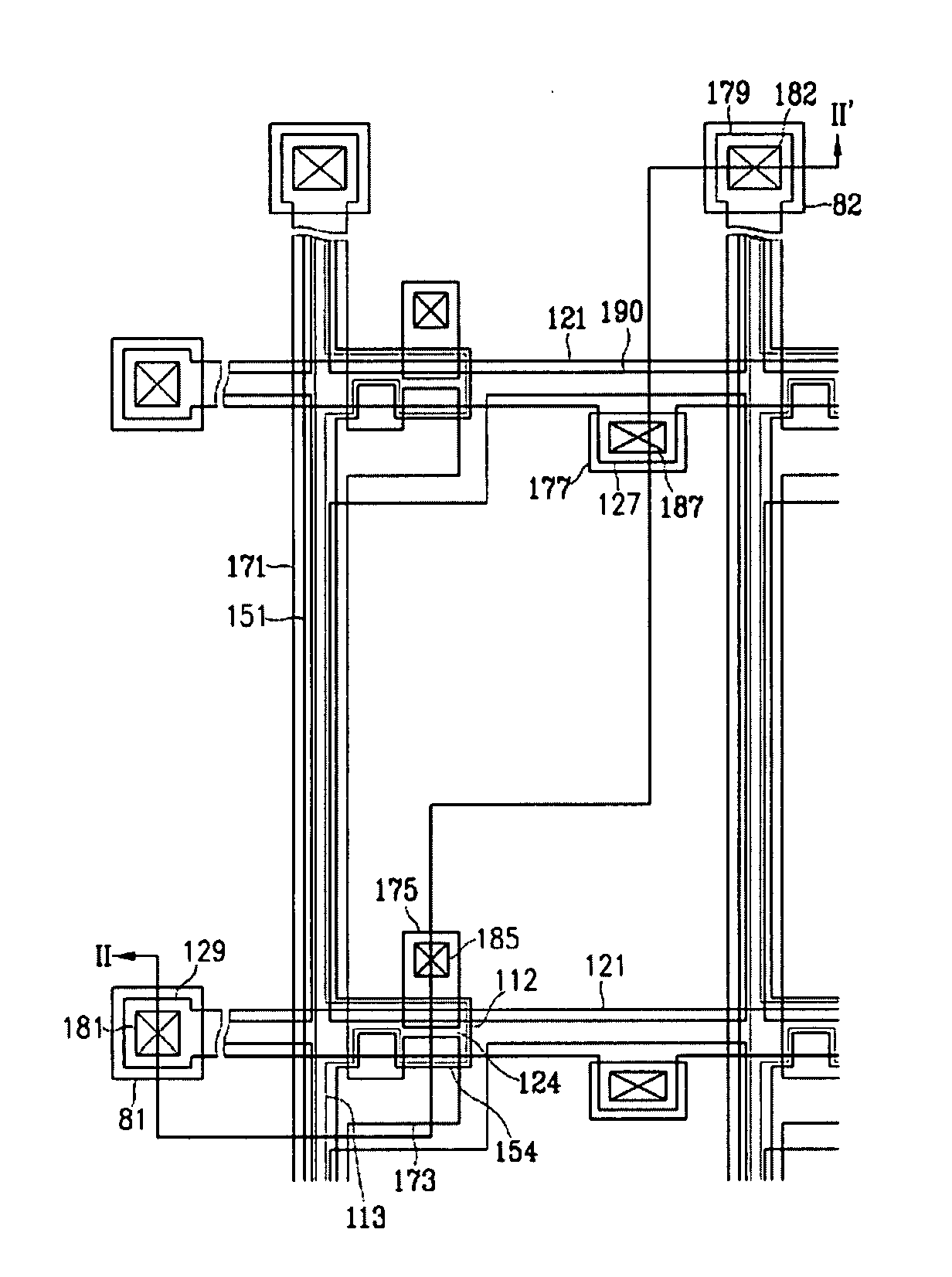
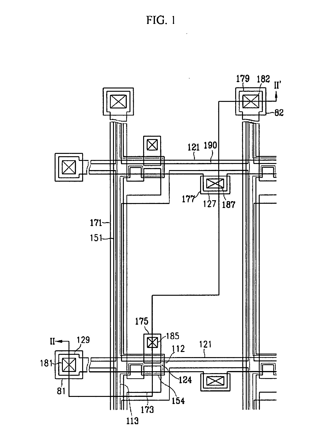
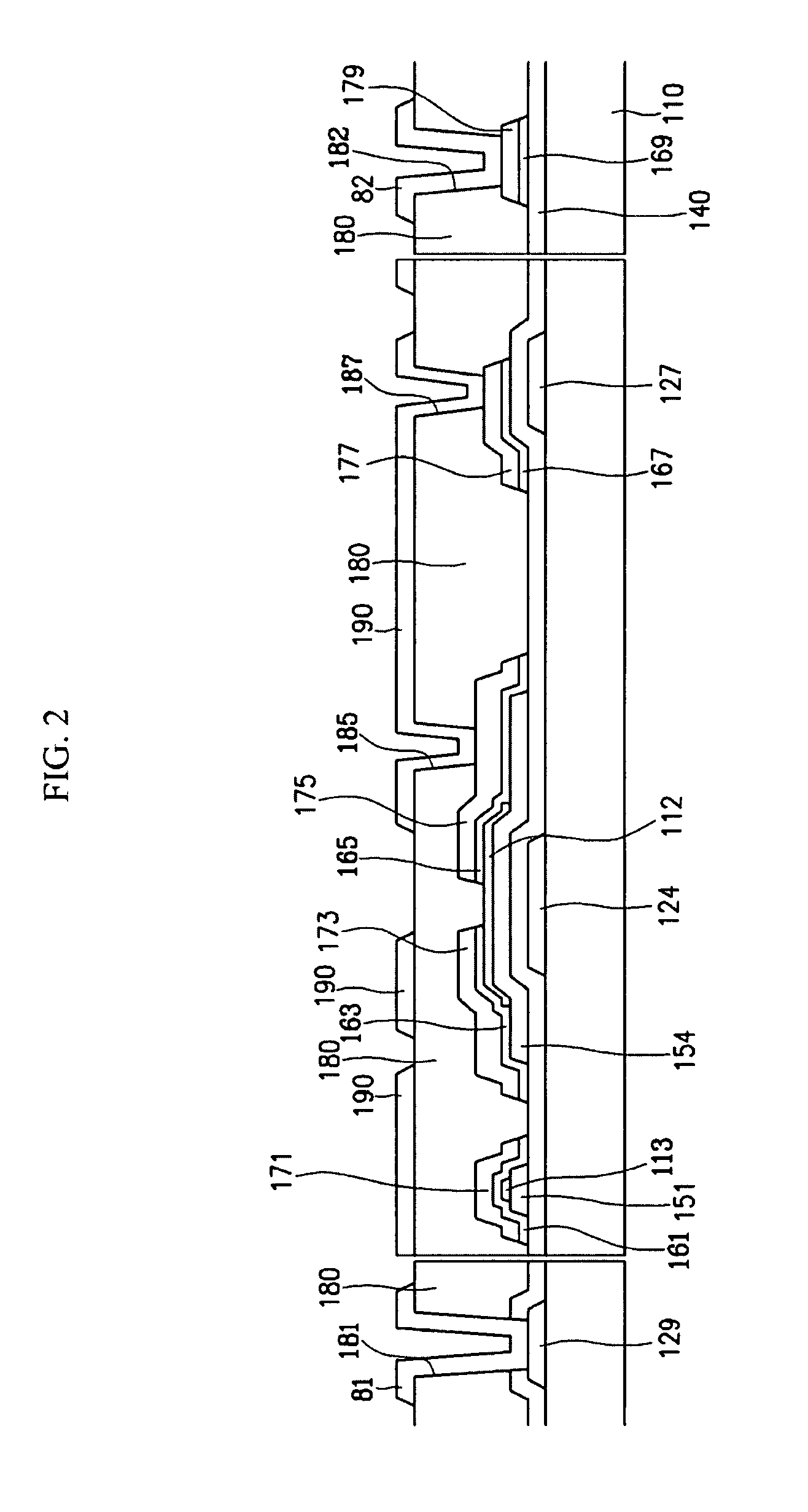
[0048]A thin film transistor array panel according to an exemplary embodiment of the present invention will be described in detail with reference to FIGS...


PUM


Abstract

A method of manufacturing a thin film transistor array panel includes forming gate lines including gate electrodes on an insulation substrate; forming a gate insulating layer, semiconductor layer, and etch stop layer on the gate lines; etching and patterning the etch stop and semiconductor layers at the same time using photolithography; ashing and partially removing a photoresist film pattern used in the patterning of the etch stop and semiconductor layers; etching the etch stop layer exposed by removed portions of the photoresist film pattern to form etch stop members; depositing ohmic contact and data metal layers onto the etch stop members, etching the ohmic contact and data metal layers at the same time using photolithography to form data lines having source and drain electrodes, and ohmic contact members below the source and drain electrodes; forming a passivation layer on the data lines and drain electrodes; and forming pixel electrodes on the passivation layer.

Description

CROSS-REFERENCE TO RELATED APPLICATION[0001]This application claims priority to Korean Patent Application No. 10-2006-0036719 filed in the Korean Intellectual Property Office on Apr. 24, 2006, the disclosure of which is incorporated by reference herein in its entirety.BACKGROUND OF THE INVENTION[0002]1. Technical Field[0003]The present invention relates to a thin film transistor array panel for a display device and a method of manufacturing the same.[0004]2. Discussion of the Related Art[0005]Liquid crystal displays are among the most widely used flat panel displays. For example, flat panel liquid crystal displays are commonly found in a variety of electronic devices such as televisions, laptop computers, personal digital assistants, cell phones and digital cameras.[0006]A liquid crystal display has two substrates on which electrodes are formed, and a liquid crystal layer interposed between the substrates. The liquid crystal display is a display device in which a voltage is applied ...

Claims


Application Information

Patent Timeline
Patent Type & Authority Applications(United States)
IPC IPC(8): H01L21/76
CPCH01L27/12H01L27/124H01L29/66765G02F1/136213G02F1/1368H01L27/1214H01L27/1255H01L27/1259
Inventor YOU, CHUN-GI
Owner SAMSUNG ELECTRONICS CO LTD
Why Eureka
Try Eureka