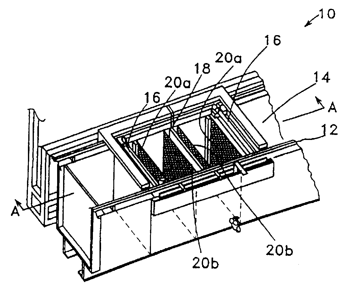
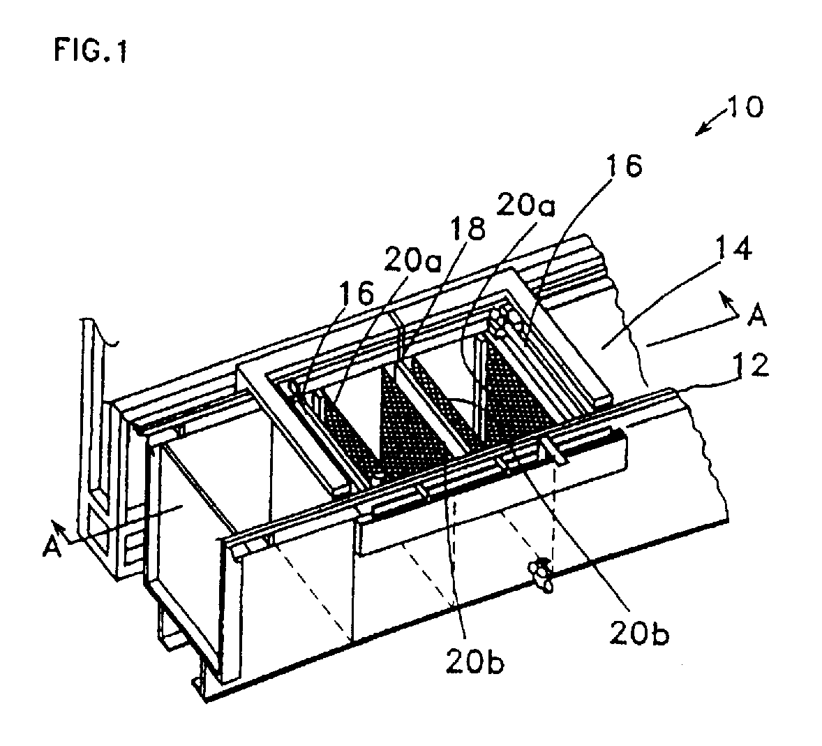
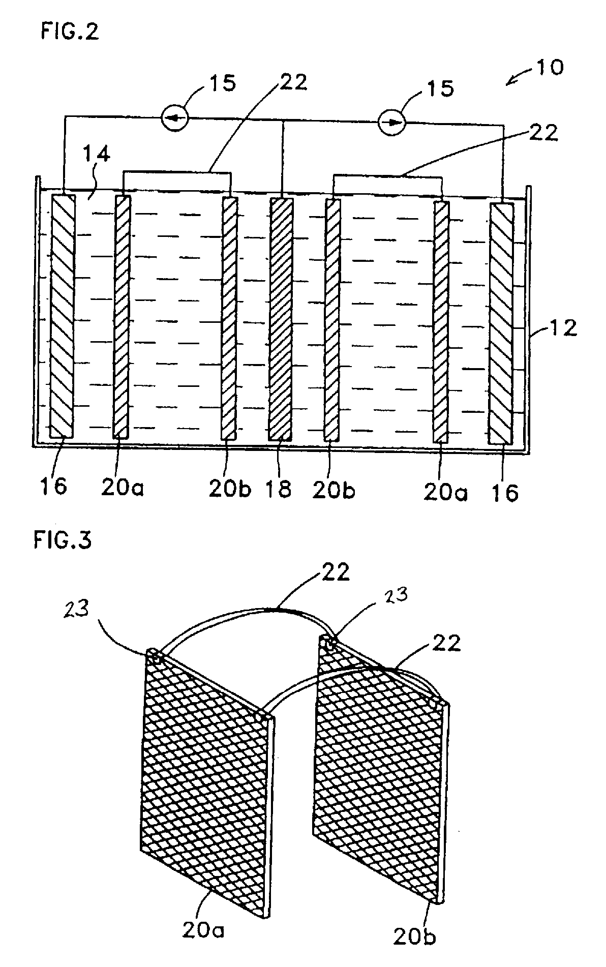
Metal plating apparatus and process
a technology of metal plating and metal plate, applied in the direction of printed element electric connection formation, cell components, non-printed masks, etc., can solve the problems of reducing production efficiency, dummy pattern reducing production efficiency, and not being able to function as an electrically productive par
- Summary
- Abstract
- Description
- Claims
- Application Information
AI Technical Summary
Benefits of technology
Problems solved by technology
Method used
Image

Examples
example 1
[0049] Plating was performed using a metal plating apparatus of the present invention equipped with conductive perforated plates. Operating conditions used were the same as those of the Comparative Example except the perforated plates were made of titanium (thickness=0.5 mm, size of hole=5 mm square, distance between the holes=0.5 mm). The spacing between the copper plate containing phosphorus and each of the perforated plates made of titanium was 1 cm, and the spacing between the circuit board and each of the perforated plates made of titanium was 1 cm. Respective portions were sampled to measure plating thickness at five sample points for plating current densities of 10 A / dm2, 6 A / dm2, 3 A / dm2, 1 A / dm2, and 0.2 A / dm2. The result is shown in FIG. 6(b).
example 2
[0050] Plating was performed using a metal plating apparatus of the present invention in which an insulating adjustment plate was laid on the conductive perforated plate made of titanium. An adjustment plate made of vinyl chloride (thickness=1 mm) was used. The windows of 0.5 mm in diameter were proportionally allocated for the respective current density based on variations in plating thickness from the average plating thickness obtained from the Comparative Example, and holes were made with a drill. The adjustment plate made of vinyl chloride was mounted on the perforated plate made of titanium with four corners fixed using clips made of vinyl chloride. The other operating conditions were similar to those of the Comparative Example. The spacing between the copper plate including phosphorus and each of the perforated plates made of titanium was 1 cm, and the spacing between the circuit board and each of the perforated plates made of titanium was 1 cm. Respective portions were sample...
PUM
| Property | Measurement | Unit |
|---|---|---|
| thickness | aaaaa | aaaaa |
| size | aaaaa | aaaaa |
| size | aaaaa | aaaaa |
Abstract
Description
Claims
Application Information
 - R&D
- Intellectual Property
- Life Sciences
- Materials
- Tech Scout
- Unparalleled Data Quality
- Higher Quality Content
- 60% Fewer Hallucinations
Browse by: Latest US Patents, China's latest patents, Technical Efficacy Thesaurus, Application Domain, Technology Topic, Popular Technical Reports.
© 2025 PatSnap. All rights reserved.Legal|Privacy policy|Modern Slavery Act Transparency Statement|Sitemap|About US| Contact US: help@patsnap.com