
Semiconductor device and fabrication method thereof

a technology of semiconductors and semiconductors, applied in the direction of semiconductor devices, basic electric elements, electrical equipment, etc., can solve the problems of increasing width, deteriorating transistor reliability, and inability to maintain transistor characteristics

Inactive Publication Date: 2008-01-24
PANASONIC CORP
View PDF0 Cites 2 Cited by
  • Summary
  • Abstract
  • Description
  • Claims
  • Application Information

AI Technical Summary

Benefits of technology

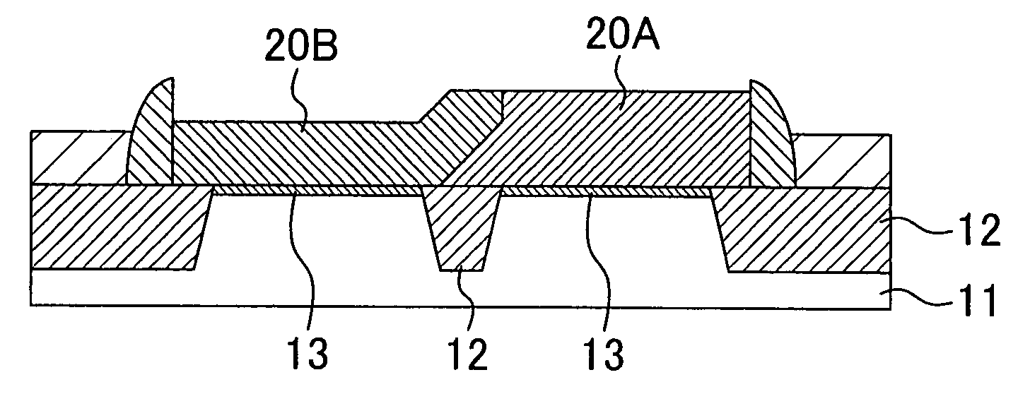
[0016]To attain the above object, a semiconductor device according to the present invention employs a dual gate electrode structure in which the interface between two silicide films having different compositions includes a tilted plane. Thus, the amount of surplus metal supplied from the part of the metal film adjoining a tilted shoulder of the stepped part of the polycrystalline silicon film can be less than the amount of surplus metal supplied from the vertical shoulder of the stepped part in the known technique. As a result, the amount of offset of the interface between the silicide films of different compositions can be reduced to less than that in the known technique. This prevents variations in transistor characteristics due to offset of the interface and in turn provides a semiconductor device including a dual gate electrode having stable transistor characteristics even when miniaturized.
[0018]With the above configuration, variations in transistor characteristics due to offset of the interface can be prevented, which provides a semiconductor device including a dual gate electrode having stable transistor characteristics even when miniaturized.
[0020]With the above configuration, a tilted plane can be easily formed in the interface between the silicide films by siliciding the polycrystalline silicon film having a tilt.

Problems solved by technology

However, if the interface reaches the N-type MIS transistor forming region A, the electric properties of the N-type MIS transistor, such as the threshold voltage, might vary, thereby providing unstable transistor characteristics and in turn deteriorating the transistor reliability.
If variations in transistor characteristics of an SRAM owing to an offset of the interface are problematic, this creates a need to increase the width of the isolation region, which prevents miniaturization of the SRAM.

Method used


Image

  • Semiconductor device and fabrication method thereof
  • Semiconductor device and fabrication method thereof
  • Semiconductor device and fabrication method thereof

Examples


embodiment 1

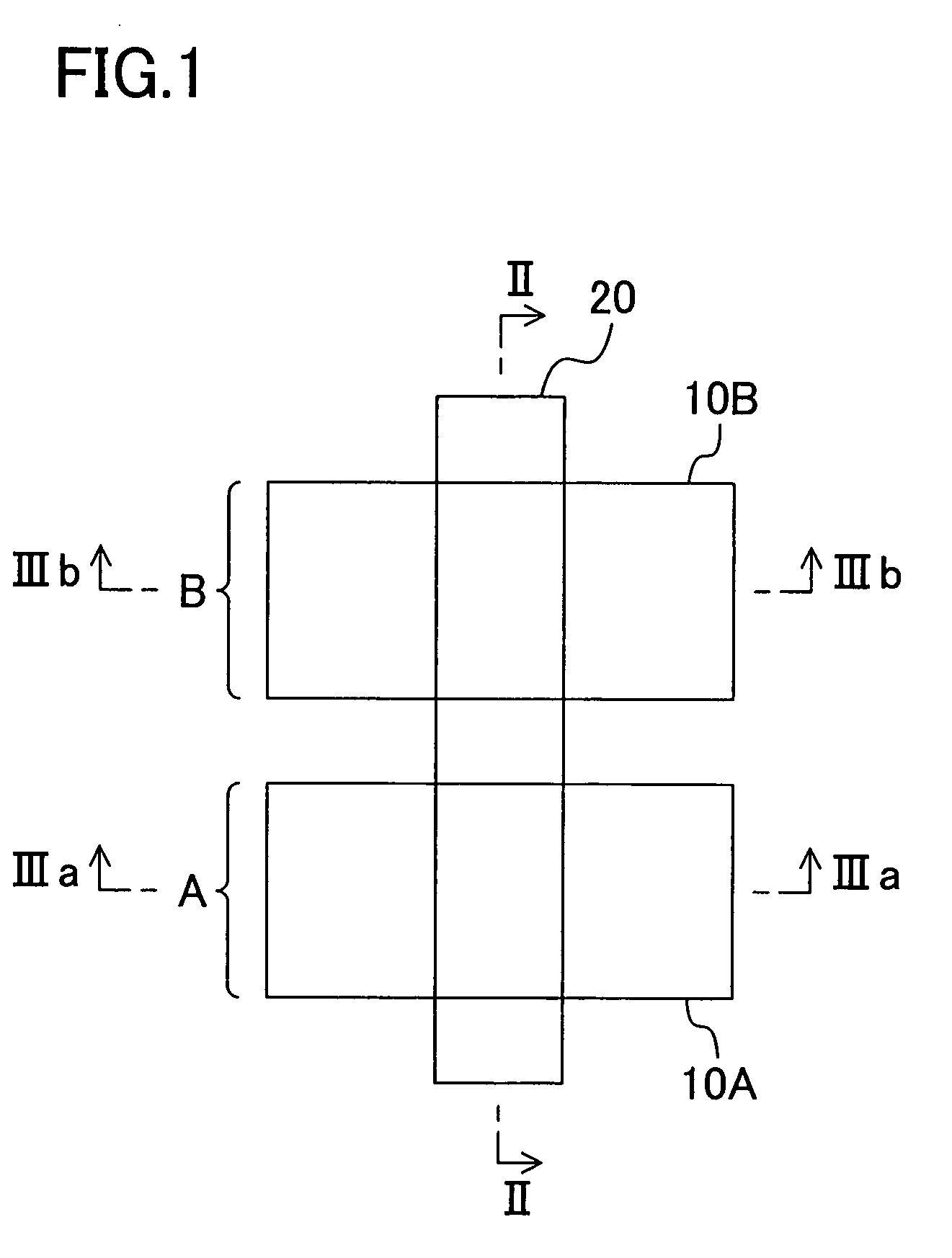
[0046]FIG. 1 is a plan view schematically showing the configuration of a semiconductor device according to a first embodiment of the present invention. As shown in the figure, a dual gate electrode 20 is formed across the top of a first element region 10A having an N-type MIS transistor formed therein and the top of a second element region 10B having a P-type MIS transistor formed therein.

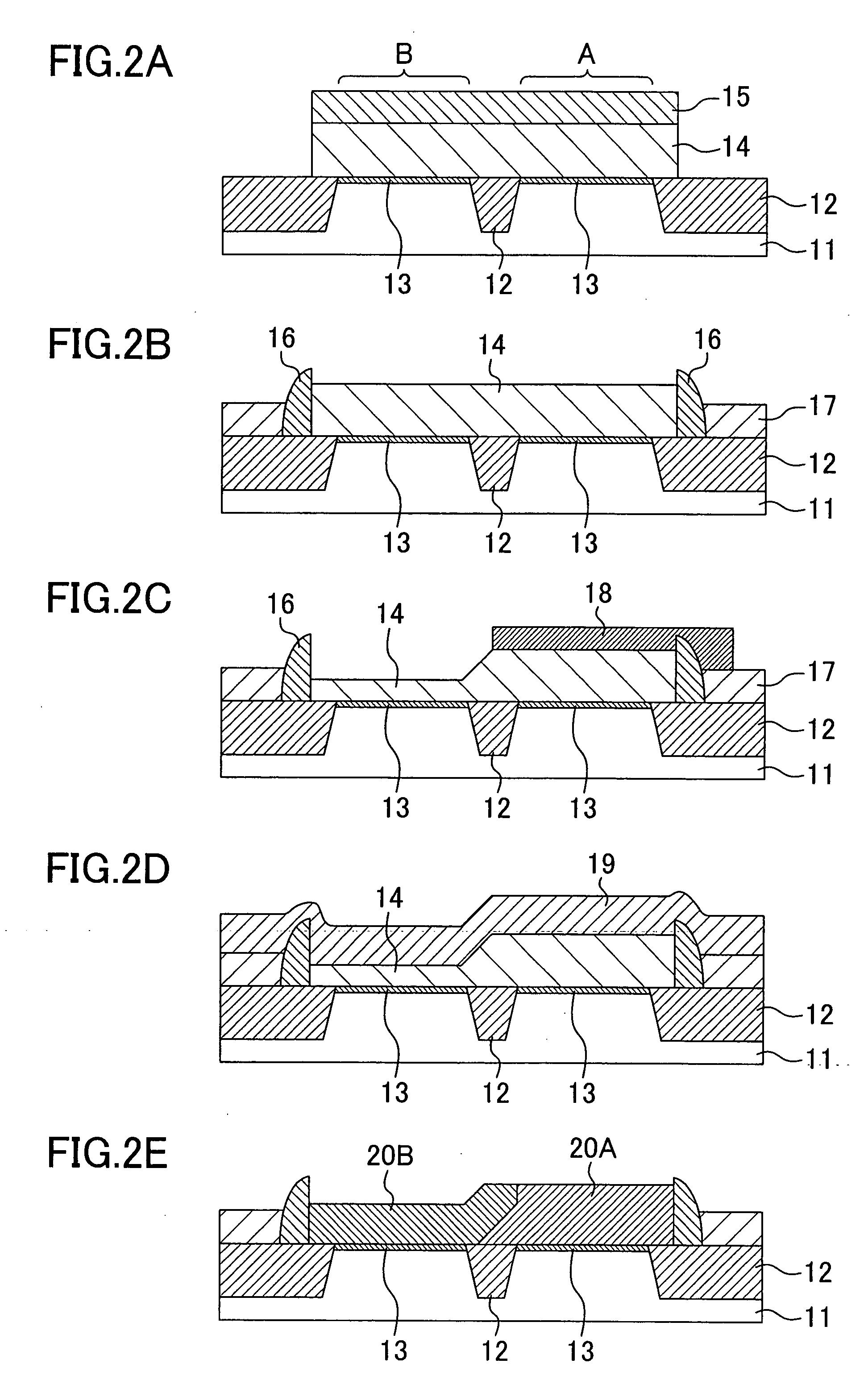
[0047]FIGS. 2A to 2E and FIGS. 3A to 3E are cross-sectional views schematically showing process steps of a method for fabricating a semiconductor device according to this embodiment, wherein FIGS. 2A to 2E are cross-sectional views taken along the line II-II of FIG. 1 and showing process steps when viewed in a direction of the gate width and FIGS. 3A to 3E are cross-sectional views taken along the line IIIa-IIIa and the line IIIb-IIIb of FIG. 1 and showing the process steps when viewed in a direction of the gate length.

[0048]The following description is given of the method for fabricating a semicon...

embodiment 2

[0059]FIGS. 4A to 5B and FIGS. 6A to 7B are cross-sectional views schematically showing process steps of a method for fabricating a semiconductor device according to a second embodiment of the present invention, wherein FIGS. 4A to 5B are, like the first embodiment, cross-sectional views taken along the line II-II of FIG. 1 and showing process steps when viewed in a direction of the gate width and FIGS. 6A to 7B are cross-sectional views taken along the line IIIa-IIIa and the line IIIb-IIIb of FIG. 1 and showing process steps when viewed in a direction of the gate length.

[0060]The following description is given of the method for fabricating a semiconductor device according to this embodiment with reference to FIGS. 4A to 5B and FIGS. 6A to 7B. Out of the process steps of the fabrication method according to this embodiment, process steps common to those shown in FIGS. 2A to 2E and FIGS. 3A to 3E are not given in detail.

[0061]First, as shown in FIGS. 4A and 6A, an isolation region 12 ...

embodiment 3

[0067]FIGS. 8A to 9B and FIGS. 10A to 11B are cross-sectional views schematically showing process steps of a method for fabricating a semiconductor device according to a third embodiment of the present invention, wherein FIGS. 8A to 9B are, like the first embodiment, cross-sectional views taken along the line II-II of FIG. 1 and showing process steps when viewed in a direction of the gate width and FIGS. 10A to 11B are cross-sectional views taken along the line IIIa-IIIa and the line IIIb-IIIb of FIG. 1 and showing process steps when viewed in a direction of the gate length.

[0068]The following description is given of the method for fabricating a semiconductor device according to this embodiment with reference to FIGS. 8A to 9B and FIGS. 10A to 11B. Out of the process steps of the fabrication method according to this embodiment, process steps common to those shown in FIGS. 2A to 2E and FIGS. 3A to 3E are not given in detail.

[0069]First, as shown in FIGS. 8A and 10A, an isolation regi...


PUM


Abstract

A semiconductor device includes a dual gate electrode lying across the tops of a first element region and a second element region formed apart from each other with an isolation region interposed between the first and second element regions. The dual gate electrode is composed of two silicide regions with different compositions: a first silicide region on top of the first element region and a second silicide region on top of the second element region. The interface between the first and second silicide regions includes a tilted plane.

Description

BACKGROUND OF THE INVENTION[0001](a) Field of the Invention[0002]This invention relates to a semiconductor device with a dual gate electrode capable of providing stable electric properties and a method for fabricating the same.[0003](b) Description of the Related Art[0004]In order to meet the recent demand for higher packing density and higher operation speed of semiconductor integrated circuits, metal alloys or high-melting point metal alloys have been employed for gate electrode wirings. Further, in order to provide a semiconductor device including an N-type MIS transistor and a P-type MIS transistor both having a low threshold voltage, a so-called dual gate electrode structure has been recently employed in which the gate electrode regions for N-type and P-type MIS transistors are formed from different materials of different work functions. For example, there is known a method for forming a dual gate electrode on N-type and P-type MIS transistors from different silicide materials ...

Claims


Application Information

Patent Timeline
Patent Type & Authority Applications(United States)
IPC IPC(8): H01L29/49H01L21/3205
CPCH01L21/28097H01L21/823835H01L29/66545H01L29/4975H01L21/823842
Inventor OHKAWA, HIROSHI
Owner PANASONIC CORP
Learn More