Method and apparatus for averaged luminance and uniformity correction in an amoled display

a technology of luminance and amoled display, applied in the direction of instruments, static indicating devices, etc., can solve the problems of variable performance of components, long-range variability of amorphous silicon devices, and significant change of threshold voltage properties of thin-film devices, so as to improve uniformity and lifetime.

Inactive Publication Date: 2007-12-20
GLOBAL OLED TECH
View PDF5 Cites 170 Cited by
  • Summary
  • Abstract
  • Description
  • Claims
  • Application Information

AI Technical Summary

Benefits of technology

[0022]In accordance with various embodiments, the present invention may

Problems solved by technology

Such thin film electronic components are subject to manufacturing process variabilities that may cause such components to have variable performance.
Amorphous silicon devices typically have a long-range variability due to variabilities in the silicon deposition processes.
Further, threshold voltage properties of such thin-film devices may changes significantly with use over time, particularly for amorphous silicon devices.
This voltage shift may result in decreased dynamic range and image artifacts.
Moreover, the organic materials in OLED devices also deteriorate in relation to the integrated current density passed through them over time so that their efficiency drops while their resistance to current increases.
However, such designs typically require complex, larger and / or slower circuits than the two-transistor, single capacitor circuits otherwise employed, thereby increasing costs and reducing the area on a display available for emitting light and decreasing the display lifetime.
However, such schemes typically require complex additional circuitry and timing signals, thereby reducing the area on a display available for emitting light and decreasing the display lifetime and cost.
However, such process steps are expensive.
However, this design also suffers from the need for additional circuitry in each active-matrix pixel.
While this technique is useful, in particular for globally compensating for behavior changes in the organic materials, it does not adequately address the problem of threshold voltage shift in active-matrix circuits.
In addition to problems relating to amorphous silicon thin-film transistors, OLED display devices suffer from a variety of defects that limit the quality of the displays.
In particular, OLED displays suffer from non-uniformities in the light-emitting elements.
These non-uniformities can be attributed to both the light emitting materials in the display and, for active-matrix displays, to variability in the thin-film transistors used to drive the light emitting elements.
However, this approach will lead to an overall reduction in the dynamic range and brightness of the display and a reduction and variation in the bit depth at which the pixels can be operated.
Moreover, such a compensation method will not address problems resulting from the aging of amorphous silicon thin-film drive transistors.
However, the described approaches require either a lookup table providing a complete characterization for each pixel, or extensive computational circuitry within a device controller.
This is likely to be expensive and impractical in most applications.
Moreover, such a compensation method will not address problems resulting from the aging of amorphous silicon thin-film drive transistors.
While brightness or luminance measurements may be practical in a manufacturing environment, and thus appropriate for initial display calibration, they may be problematic after the display is subsequently put into use and thus less practical for performance of aging compensation.
WO 2005 / 057544 describes a video data signal correction system for video data signals addressing active matrix electroluminescent display devices wherein an updated electrical characteristic parameter X is calculated for each drive transistor by measuring actual current through a power line in comparison to expected current determined using a model and a previously stored parameter value, where subsequent video data signals are corrected in accordance with the calculated parameter X. Calculation of characteristic parameters based on assumed pre-determined performance relationships, however, may require consideration of many parameters having complex interactive relationships, and further may not accurately reflect actual device performance.

Method used


Image

  • Method and apparatus for averaged luminance and uniformity correction in an amoled display
  • Method and apparatus for averaged luminance and uniformity correction in an amoled display
  • Method and apparatus for averaged luminance and uniformity correction in an amoled display

Examples


Embodiment Construction

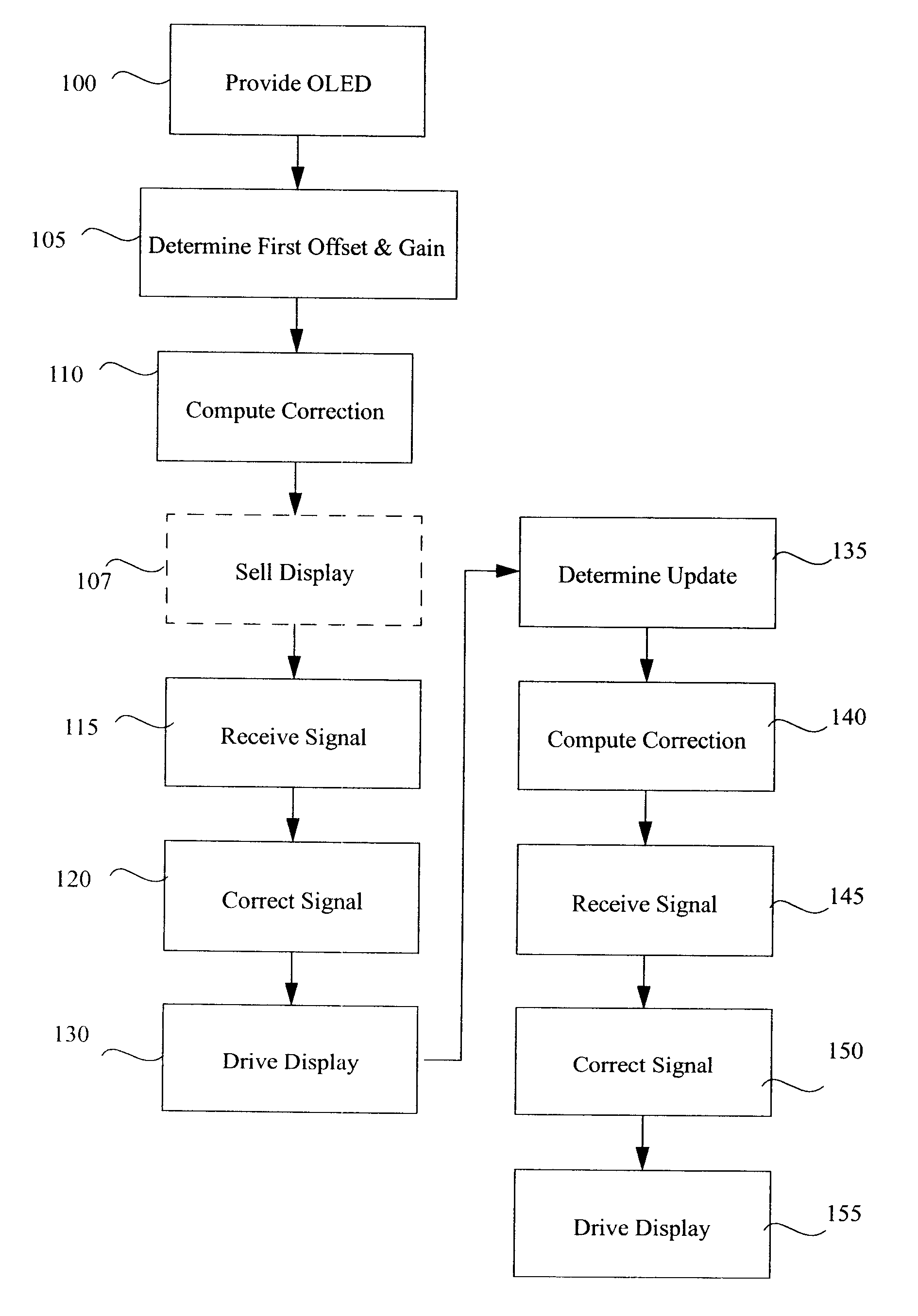
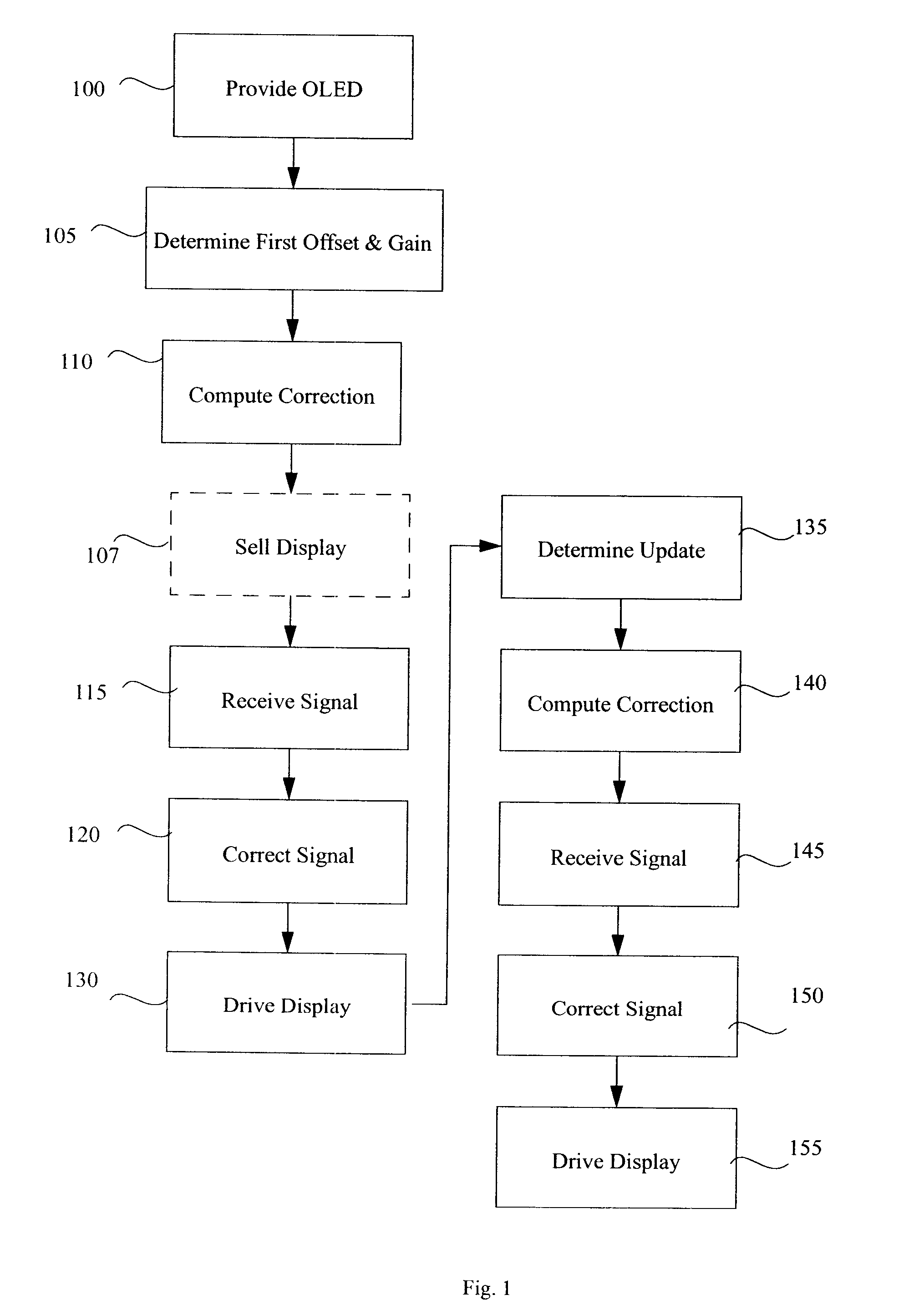
[0031]Referring to FIG. 1, a method for the correction of average luminance or luminance uniformity variations in an active-matrix OLED display comprises the steps of providing 100 an active-matrix OLED display having thin-film transistors driving one or more light-emitting elements responsive to a multi-valued input signal for causing the light-emitting elements to emit light at a plurality of brightness levels; determining 105 at a first time a first offset voltage at which at least one of the one or more light-emitting elements will not conduct more than a pre-determined minimum current and a first gain relationship between the voltage and the current passing through the at least one of the one or more light-emitting elements at voltages above the first offset voltage; receiving 115 a signal for driving the one or more light-emitting elements after determining the first offset voltage and first gain relationship, correcting the signal by employing the first offset voltage and gai...


PUM


Abstract

A method for the correction of average luminance or luminance uniformity variations in an active-matrix OLED display, comprising:a) providing an active-matrix OLED display;b) determining at a first time a first offset voltage and a first gain relationship between the voltage and the current passing through one or more light-emitting elements;c) receiving a signal for driving the light-emitting elements after step b), correcting the signal by employing the first offset voltage and gain relationship values to compute a linear correction for the light-emitting elements to form a corrected signal, and driving the display with the corrected signal;d) determining at a time after the first time an updated offset voltage and an updated gain relationship between the voltage and the current passing through the light-emitting elements; ande) receiving a signal for driving the one or more light-emitting elements after step d), correcting the signal by employing the updated offset voltage and gain relationship values to compute a linear correction for the light-emitting elements to form an updated corrected signal, and driving the display with the updated corrected signal.

Description

FIELD OF THE INVENTION[0001]The present invention relates to active-matrix OLED displays employing thin-film transistors and having a plurality of light-emitting elements and, more particularly, methods and apparatus for correcting average luminance and luminance uniformity of the light-emitting elements in such displays, including displays employing amorphous silicon thin-film transistors.BACKGROUND OF THE INVENTION[0002]Flat-panel display devices, for example plasma, liquid crystal and Organic Light Emitting Diode (OLED) displays have been known for some years and are widely used in electronic devices to display information and images. Such devices employ both active-matrix and passive-matrix control schemes and can employ a plurality of light-emitting elements. The light-emitting elements are typically arranged in two-dimensional arrays with a row and a column address for each light-emitting element and having a data value associated with each light-emitting element to emit light...

Claims


Application Information

Patent Timeline
IPC IPC(8): G09G3/30
CPCG09G3/3225G09G2320/043G09G2320/029G09G2320/0285
Inventor COK, RONALD S.
Owner GLOBAL OLED TECH
Why Eureka
Try Eureka