
Method for Manufactuing a Semiconductor Integrated Circuit Device

a manufacturing method and semiconductor technology, applied in semiconductor/solid-state device testing/measurement, semiconductor/solid-state device details, instruments, etc., can solve the problems of loss of electrical continuity between bump electrodes and corresponding pads, undue contact resistance between the two kinds of electrodes, etc., to achieve high-reliability semiconductor integrated circuit devices

Inactive Publication Date: 2007-12-13
RENESAS TECH CORP
View PDF7 Cites 12 Cited by
  • Summary
  • Abstract
  • Description
  • Claims
  • Application Information

AI Technical Summary

Benefits of technology

[0004] To secure good electrical continuity with the external connection terminals of the package, the socket board (tape board) which is used for the burn-in test is designed and manufactured for each type of package in accordance with the shape and the number of pins of the external connection terminals.
[0105] An advantage obtained by the typical aspects of the invention disclosed in this application will be described briefly. That is, it becomes possible to perform a burn-in test on a semiconductor integrated circuit device having high-density bump electrodes and to thereby provide highly reliable semiconductor integrated circuit devices.

Problems solved by technology

Therefore, the contact resistance between the two kinds of electrodes may become unduly large or electrical continuity between part of the bump electrodes and corresponding pads may be lost due to a variation in the diameter of the bump electrodes.

Method used


Image

  • Method for Manufactuing a Semiconductor Integrated Circuit Device
  • Method for Manufactuing a Semiconductor Integrated Circuit Device
  • Method for Manufactuing a Semiconductor Integrated Circuit Device

Examples


Embodiment Construction

[0136] An embodiment of the present invention will be hereinafter described in detail with reference to the drawings. In all drawings for the description of the embodiment, the same members are basically given the same reference symbol and will not be described repeatedly.

[0137] Before the detailed description of the invention, terms used in this application will be described. The term “semiconductor wafer” covers a silicon single crystal substrate (in general, approximately flat and circular) used for manufacture of integrated circuits, a sapphire substrate, a glass substrate, other insulative, semi-insulative, or semiconductor substrates, and composite substrates thereof. The term “semiconductor integrated circuit device” as used in this application not only covers ones formed on a semiconductor or insulator substrate such as a silicon wafer or a sapphire substrate but also covers, unless otherwise specified, ones formed on other kinds of insulator substrates such as a glass subs...


PUM


Abstract

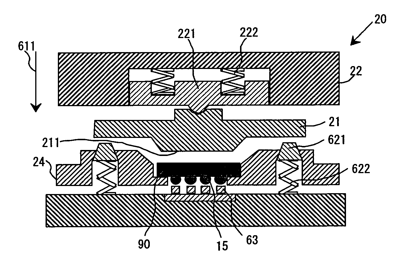
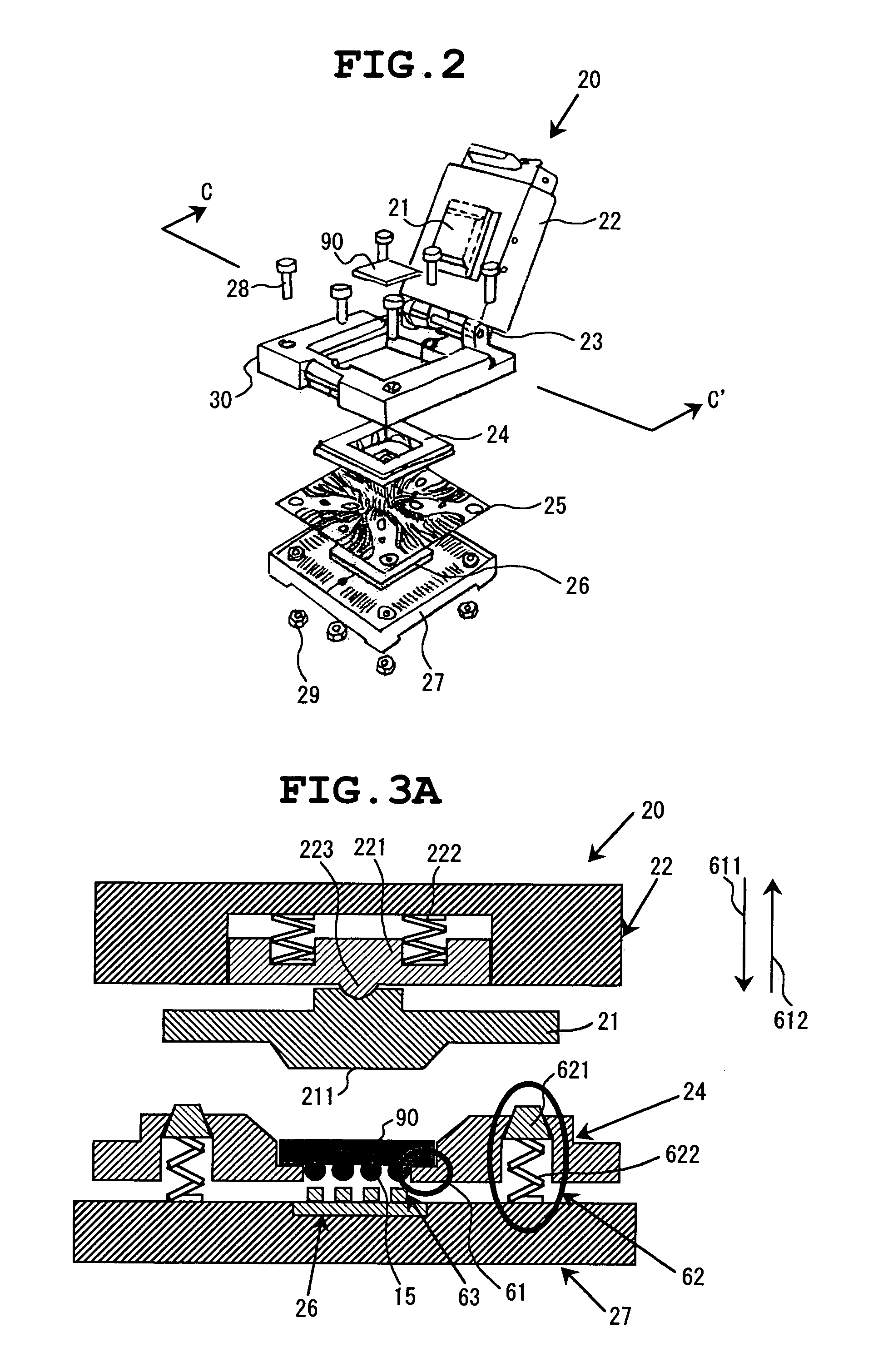
A burn-in process for a semiconductor integrated circuit device includes a first process of positioning bump electrodes of the semiconductor integrated circuit device with respect to pads of a socket having detachment mechanisms, a second process of pressing the bump electrodes against the pads by weighting the semiconductor integrated circuit device, and a third process of detaching the bump electrodes from the pads by exerting force on the semiconductor integrated circuit device in a direction opposite to a weighting direction of the second process. Automatic insertion and detachment of a semiconductor integrated circuit chip in a burn-in test is facilitated by detaching the bump electrodes from the pads by pushing up the semiconductor integrated circuit device.

Description

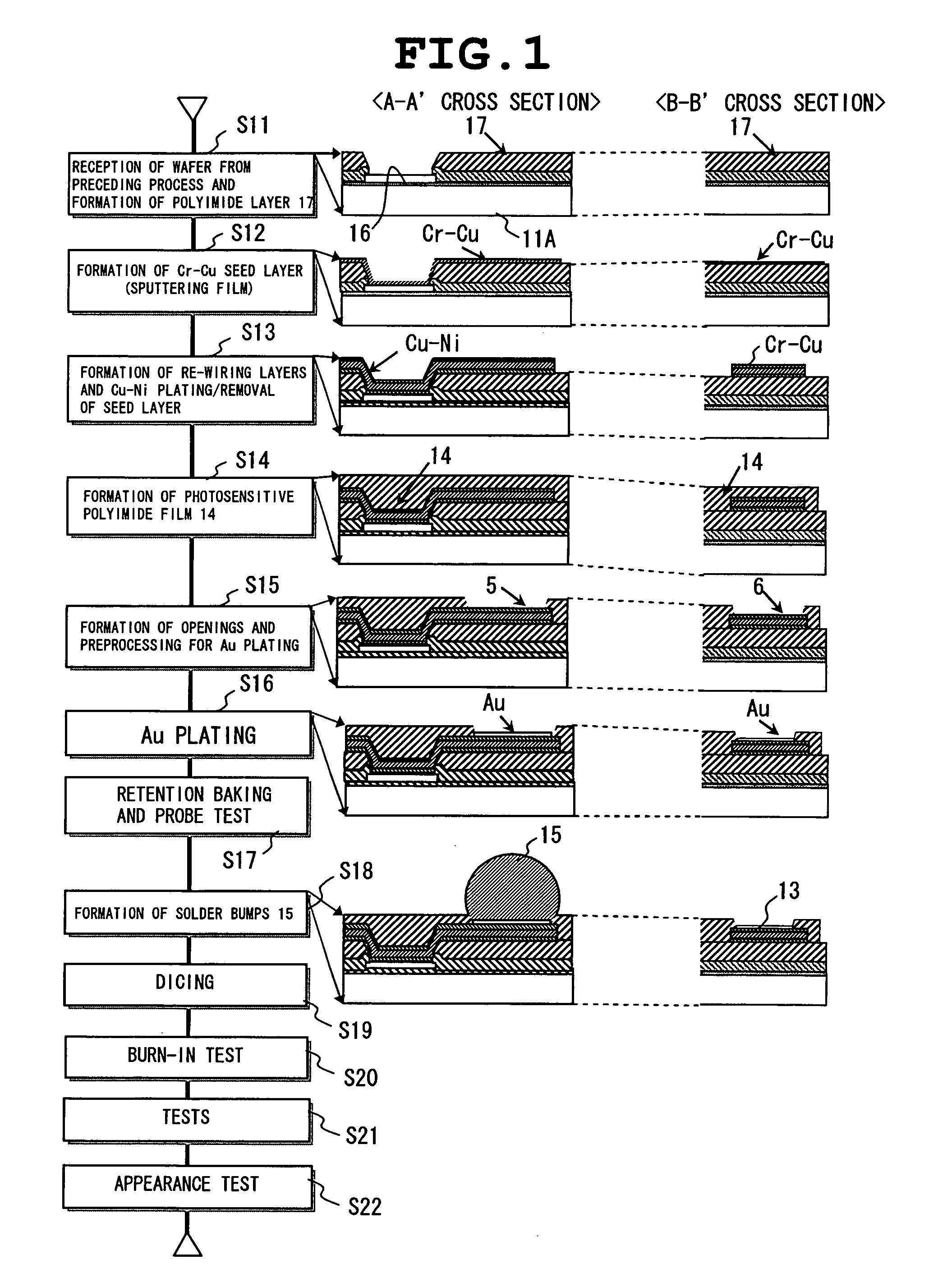
FIELD OF THE INVENTION [0001] The present invention relates to a technique for manufacturing a semiconductor device. For example, the invention relates to a technique which is effectively applied to attachment / detachment of a semiconductor device having bump electrodes as external connection terminals to / from a burn-in (accelerated energization) test apparatus. BACKGROUND OF THE INVENTION [0002] JP-A-2000-235062 (FIG. 1 etc.) discloses an improvement of electrodes of a burn-in test socket (also referred to simply as “socket”) which are brought in contact with bump electrodes of a semiconductor integrated circuit device (semiconductor device) in a burn-in test of the semiconductor integrated circuit device. SUMMARY OF THE INVENTION [0003] In manufacturing processes of semiconductor integrated circuits, to remove defective products and measure product lifes, chips that have been obtained by dicing a wafer and sealed in packages are subjected to a burn-in test before shipment. The burn...

Claims


Application Information

Patent Timeline
Patent Type & Authority Applications(United States)
IPC IPC(8): G01R31/26H01L21/66G01R1/04G01R31/28
CPCG01R1/0483G01R31/2863H01L24/11H01L2924/13091H01L2924/00H01L2924/14H01L23/48
Inventor MAKIHARA, NAOHIROIMASU, SATOSHISATO, MASANAO
Owner RENESAS TECH CORP
Learn More