
Apparatus for integration of barrier layer and seed layer

a technology of which is applied in the field of apparatus for depositing barrier layer and seed layer, can solve the problems of compromising device integrity, affecting the integrity of devices, and requiring a large amount of ongoing effor

Inactive Publication Date: 2007-12-13
APPLIED MATERIALS INC
View PDF99 Cites 24 Cited by
  • Summary
  • Abstract
  • Description
  • Claims
  • Application Information

AI Technical Summary

Benefits of technology

This approach enhances the reliability of copper interconnects by ensuring continuous seed layer formation, reducing the likelihood of voids and agglomeration, and maintaining device integrity under thermal stress, effectively addressing the limitations of traditional barrier layers.

Problems solved by technology

However, as the fringes of circuit technology are pressed, the shrinking dimensions of interconnects in VLSI and ULSI technology have placed additional demands on the processing capabilities.
Many traditional deposition processes have difficulty filling sub-micron structures where the aspect ratio exceeds 4:1, and particularly where the aspect ratio exceeds 10:1.
Therefore, there is a great amount of ongoing effort being directed at the formation of substantially void-free and seam-free sub-micron features having high aspect ratios.
However, one problem with the use of copper is that copper diffuses into silicon, silicon dioxide, and other dielectric materials which may compromise the integrity of devices.
One problem with prior uses of tantalum nitride and other barrier layers, however, is that these barrier layers are poor wetting agents for the deposition of copper thereon which may cause numerous problems.
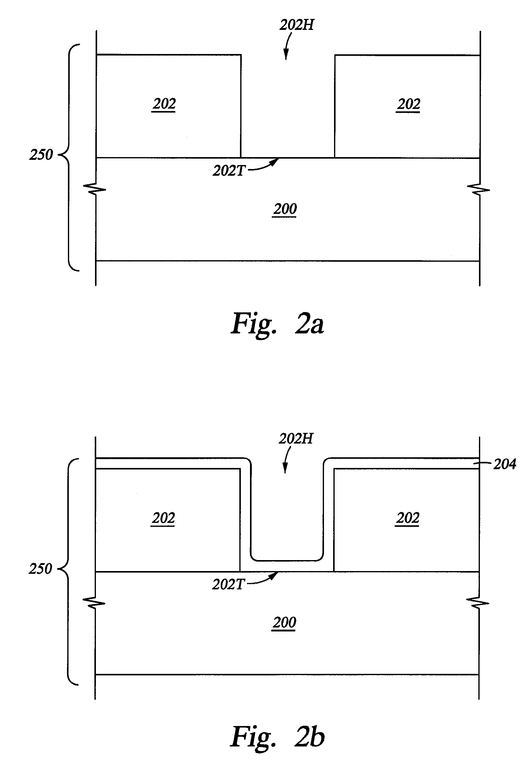
For example, during deposition of a copper seed layer over these barrier layers, the copper seed layer may agglomerate and become discontinuous, which may prevent uniform deposition of a copper conductive material layer (i.e., electroplating of a copper layer) over the copper seed layer.
In another example, subsequent processing at high temperatures of a substrate structure having a copper layer deposited over these barrier layers may cause dewetting and the formation of voids in the copper layer.
In still another example, thermal stressing of formed devices through use of the devices may cause the generation of voids in the copper layer and device failure.

Method used


Image

  • Apparatus for integration of barrier layer and seed layer
  • Apparatus for integration of barrier layer and seed layer
  • Apparatus for integration of barrier layer and seed layer

Examples


example 1

[0078] A TaN layer was deposited over a substrate by atomic layer deposition to a thickness of about 20 Å. A seed layer was deposited over the TaN layer by physical vapor deposition to a thickness of about 100 Å. The seed layer comprised either 1) undoped copper deposited utilizing a target comprising undoped copper, 2) a copper alloy comprising aluminum in a concentration of about 2.0 atomic percent deposited utilizing a copper-aluminum target comprising aluminum in a concentration of about 2.0 atomic percent, 3) a copper alloy comprising tin in a concentration of about 2.0 atomic percent deposited utilizing a copper-tin target comprising tin in a concentration of about 2.0 atomic percent, or 4) a copper alloy comprising zirconium in a concentration of about 2.0 atomic percent deposited utilizing a copper-zirconium target comprising zirconium in a concentration of about 2.0 atomic percent. The resulting substrate was annealed at a temperature of about 380° C. for a time period of a...

example 2

[0080] Copper-aluminum alloy films comprising about 2.0 atomic percent of aluminum were deposited on different substrates by physical vapor deposition utilizing a copper-aluminum target comprising aluminum in a concentration of 2.0 atomic percent. The resulting substrates included 1) a copper-aluminum layer deposited to a thickness of about 50 Å over an ALD TaN layer, 2) a copper-aluminum layer deposited to a thickness of about 50 Å over about a 100 Å Ta layer, 3) a copper-aluminum layer deposited to a thickness of about 100 Å over an ALD TaN layer, 4) a copper-aluminum layer deposited to a thickness of about 100 Å over a silicon nitride (SiN) layer, and 5) a copper-aluminum layer deposited to a thickness of about 100 Å over a silicon oxide layer. The resulting substrates were annealed at a temperature of about 380° C. for a time period of about 15 minutes in a nitrogen (N2) and hydrogen (H2) ambient. Scanning electron microscope photographs showed that there was no significant aggl...

example 3

[0081] Copper-aluminum alloy films comprising about 2.0 atomic percent of aluminum were deposited by physical vapor deposition utilizing a copper-aluminum target comprising aluminum in a concentration of 2.0 atomic percent to either a 50 Å or 100 Å thickness over an ALD TaN layer. The resulting substrates were annealed at a temperature of about 380° C., about 450° C., or about 500° C. for a time period of about 15 minutes in a nitrogen (N2) and hydrogen (H2) ambient. Scanning electron microscope photographs showed that there was no significant agglomeration of the copper-aluminum alloy for substrates annealed at temperatures of about 380° C. or about 450° C. The copper-aluminum alloy showed some dewetting began to occur for substrates annealed at a temperature of about 500° C.


PUM

PropertyMeasurementUnit
temperatureaaaaaaaaaa
temperaturesaaaaaaaaaa

Abstract

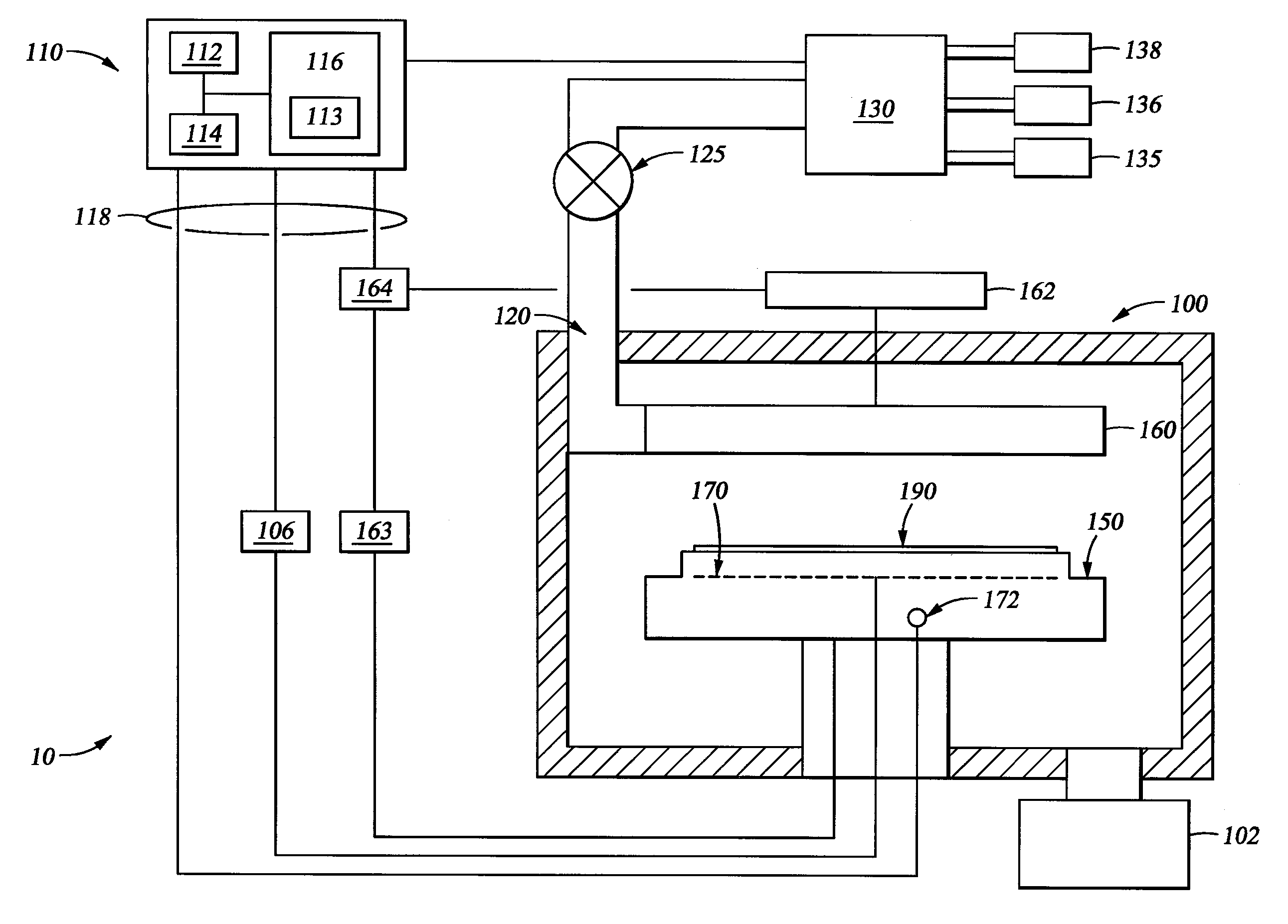
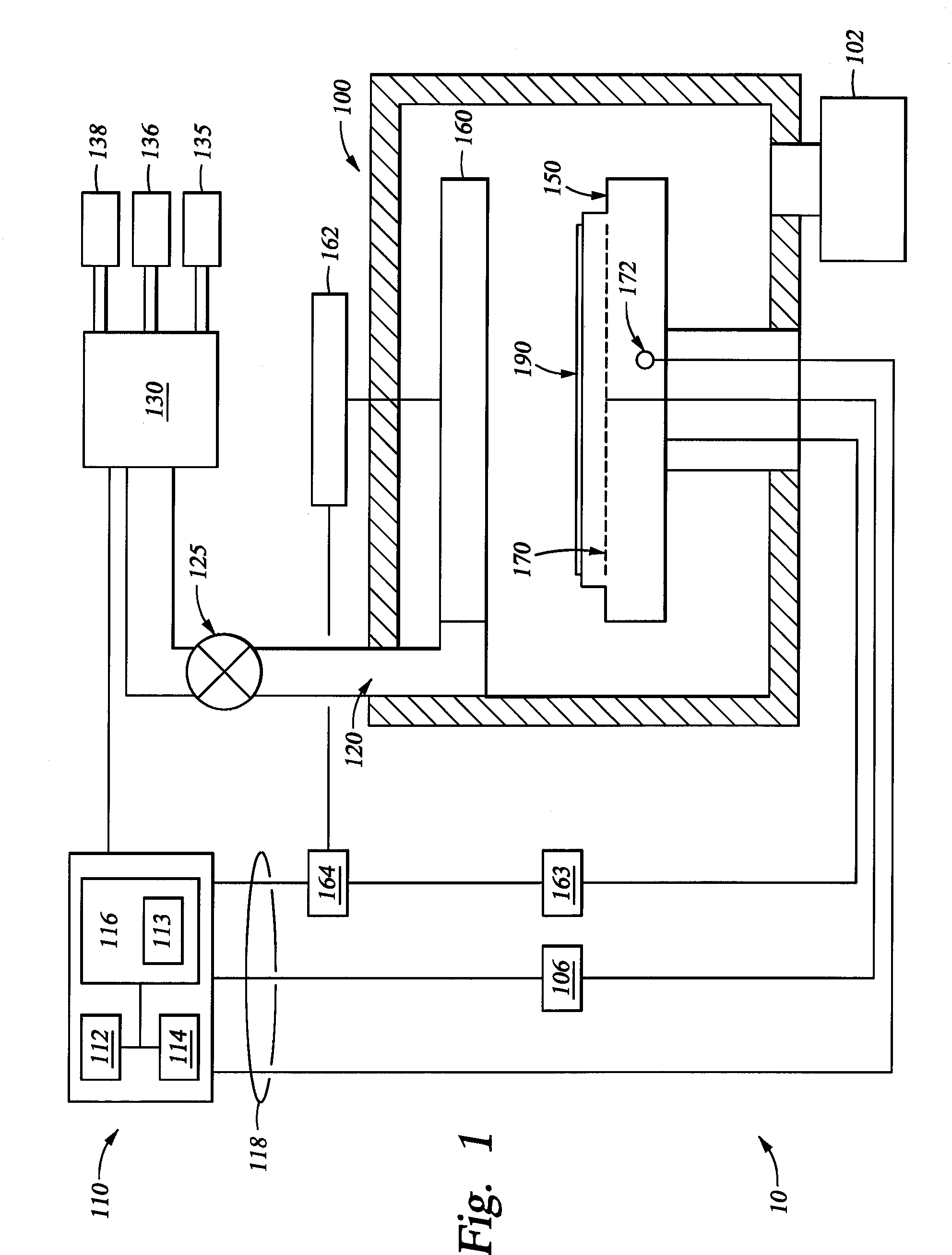
A system for processing a substrate is provided which includes at least one atomic layer deposition (ALD) chamber for depositing a barrier layer containing tantalum and at least one physical vapor deposition (PVD) metal seed chamber for depositing a metal seed layer on the barrier layer. The at least one ALD chamber may be in fluid communication with a first precursor source providing a tantalum-containing compound and a second precursor source. In one example, the tantalum-containing compound is an organometallic tantalum precursor, such as PDMAT. In another example, the second precursor source contains a nitrogen precursor, such as ammonia. The PDMAT may have a chlorine concentration of about 100 ppm or less, preferably, about 30 ppm or less, and more preferably, about 5 ppm or less. In some examples, the PVD metal seed chamber is used to deposit a copper-containing metal seed layer.

Description

CROSS-REFERENCE TO RELATED APPLICATIONS [0001] This application is a continuation of U.S. Ser. No. 11 / 064,274 (APPM / 006303.C1), filed Feb. 22, 2005, which is a continuation of U.S. Ser. No. 09 / 965,373 (APPM / 006303.02), filed Sep. 26, 2001, and issued as U.S. Pat. No. 6,936,906, which are herein incorporated by reference in their entirety.BACKGROUND OF THE INVENTION [0002] 1. Field of the Invention [0003] Embodiments of the invention generally relate to an apparatus and method for depositing a barrier layer and a seed layer thereon, and more particularly, to an apparatus and method for depositing a barrier layer containing tantalum and depositing a seed layer containing copper or other metals. [0004] 2. Description of the Related Art [0005] Reliably producing sub-micron and smaller features is one of the key technologies for the next generation of very large scale integration (VLSI) and ultra large scale integration (ULSI) of semiconductor devices. However, as the fringes of circuit ...

Claims


Application Information

Patent Timeline
Patent Type & Authority Applications(United States)
IPC IPC(8): C23C16/00C23C14/34C23C16/34H01L21/285H01L21/768H01L23/532H01L23/58H01L27/095
CPCC23C14/046Y10S438/903C23C14/3414C23C16/045C23C16/34C23C16/45525H01L21/2855H01L21/28562H01L21/76843H01L21/76846H01L21/76862H01L21/76864H01L21/76871H01L23/53238H01L2221/1089C23C14/165H01L2924/0002H01L2924/00
Inventor CHUNG, HUACHEN, LINGYU, JICKCHANG, MEI
Owner APPLIED MATERIALS INC
Learn More