
Patterning process and method of manufacturing organic thin film transistor using the same

a technology patterning process, which is applied in the direction of basic electric elements, electrical apparatus, semiconductor devices, etc., can solve the problems of increasing the difficulty of high precision, reducing the performance of organic thin film transistor b>100/b>, and creating additional problems, etc., to achieve the effect of greater pattern precision

Inactive Publication Date: 2007-11-15
CHUNGHWA PICTURE TUBES LTD
View PDF17 Cites 14 Cited by
  • Summary
  • Abstract
  • Description
  • Claims
  • Application Information

AI Technical Summary

Benefits of technology

[0008] Accordingly, at least one objective of the present invention is to provide a patterning process capable of defining a pattern with a greater pattern precision.
[0009] At least another objective of the present invention is to provide a method of manufacturing an organic thin film transistor capable of improving interface characteristic of an organic semiconductor layer in an active region and defining an organic thin film channel layer with a greater pattern precision.
[0031] The patterning process in the present invention uses a patterned self-assembled monolayer to define the organic semiconductor layer. Therefore, the device can be defined with a greater pattern precision and the interface characteristic of the organic semiconductor layer can be improved. Furthermore, using the patterning process of the present invention to manufacture the organic thin film transistor also improves the interface characteristic of the organic semiconductor layer within the active region and defines the organic semiconductor layer with a greater pattern precision.

Problems solved by technology

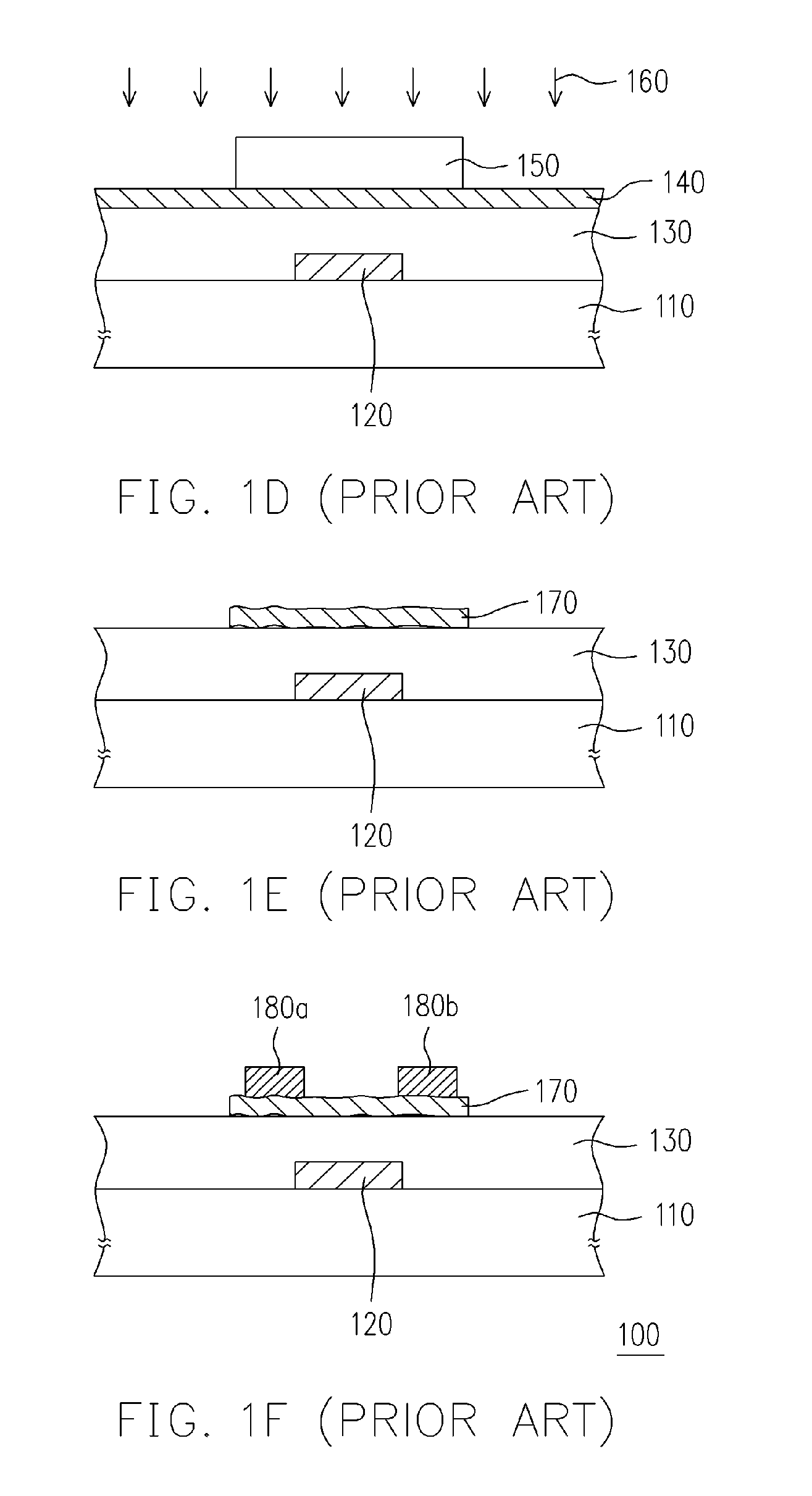
Furthermore, using the patterned photoresist 150 as a mask to pattern the organic material layer 140 in the etching process 160 may create additional problems.
More specifically, because the patterned photoresist 150 is used as a mask to remove the unprotected organic material layer 140, the pattern in an active region (that is, the organic semiconductor layer 170) having a very high precision is difficult to obtained, such that the performance of the organic thin film transistor 100 may drop and the leakage current in the active region may be excessively large.

Method used


Image

  • Patterning process and method of manufacturing organic thin film transistor using the same
  • Patterning process and method of manufacturing organic thin film transistor using the same
  • Patterning process and method of manufacturing organic thin film transistor using the same

Examples


Embodiment Construction

[0039] Reference will now be made in detail to the present preferred embodiments of the invention, examples of which are illustrated in the accompanying drawings. Wherever possible, the same reference numbers are used in the drawings and the description to refer to the same or like parts.

[0040] The patterning process and the method of forming the organic thin film transistor in the present invention utilizes a self-assembled monolayer to define an organic material layer with a greater pattern precision. Furthermore, the interface characteristic of the organic material layer is also improved through the self-assembled monolayer. The following illustrations are just some of the preferred embodiments of the present invention and should not be used to limit the scope of the present invention.

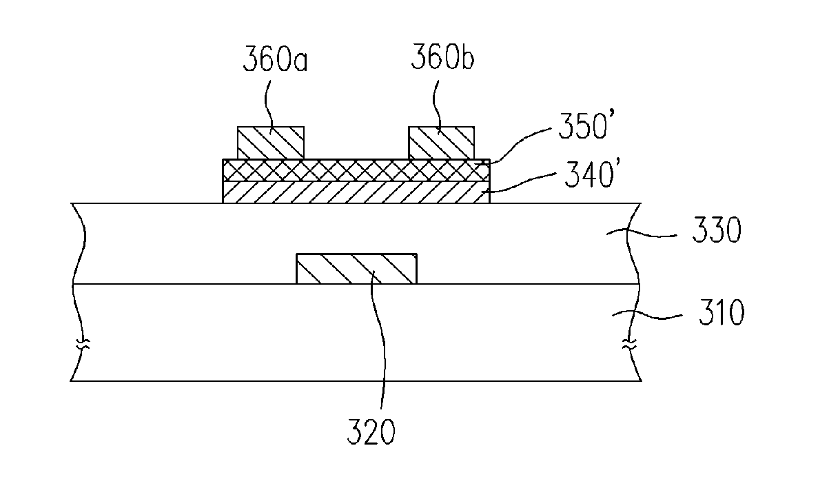
[0041]FIGS. 2A through 2G are schematic cross-sectional views showing the steps in a patterning process according to one preferred embodiment of the present invention. First, as shown in FIG. 2A, ...


PUM

PropertyMeasurementUnit
organicaaaaaaaaaa
semiconductoraaaaaaaaaa
flexibleaaaaaaaaaa

Abstract

A patterning process is provided. The patterning process includes the following steps. First, a substrate is provided. Then, a patterned self-assembled monolayer (SAM) is formed on the substrate. Afterwards, an organic material layer is formed over the substrate to cover the self-assembled monolayer. Thereafter, a portion of the organic material layer is removed, wherein the organic material layer in contact with the patterned SAM is retained such that a patterned organic material layer.

Description

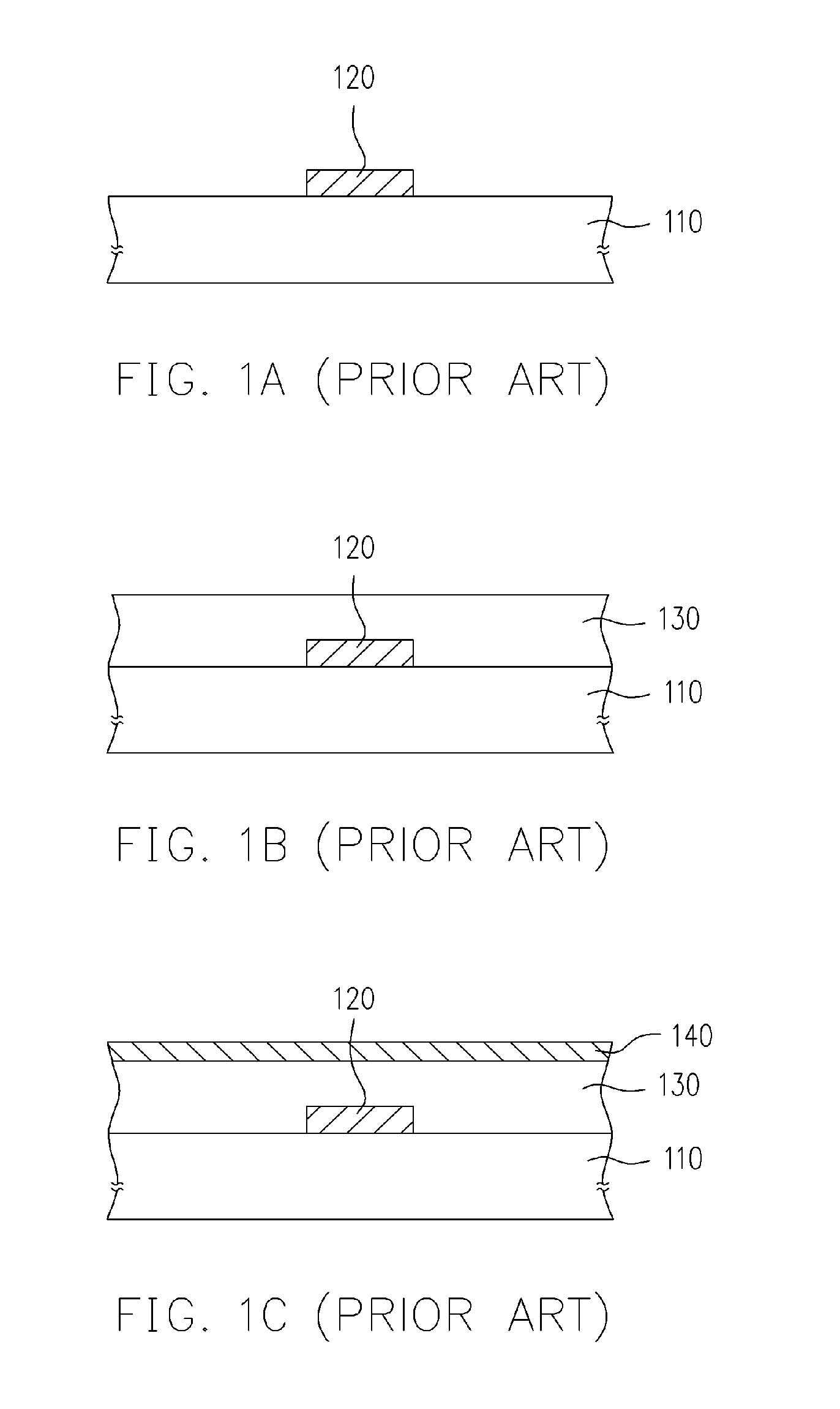
BACKGROUND OF THE INVENTION [0001] 1. Field of the Invention [0002] The present invention relates to a patterning process and a method of manufacturing an organic thin film transistor using the same. More particularly, the present invention relates to a patterning process using a self-assembled monolayer (SAM) and a method of manufacturing an organic thin film transistor (O-TFT) using the patterning process. [0003] 2. Description of Related Art [0004] Because organic semiconductor devices can be fabricated on a flexible plastics substrate or a thin metal substrate, it has the advantages of being light, cheap and flexible. Among the organic semiconductor devices, organic thin film transistor (O-TFT) has become one of the most important devices both in the academic circle and among industrial researchers in technically advanced countries. [0005]FIGS. 1A through 1F are schematic cross-sectional views showing the steps of fabricating a conventional organic thin film transistor. First, a...

Claims


Application Information

Patent Timeline
Patent Type & Authority Applications(United States)
IPC IPC(8): H01L51/40
CPCH01L51/0017H01L51/0541H01L51/0055H10K71/231H10K85/623H10K10/464
Inventor YEN, KUO-HSICHOU, CHENG-WEIZAN, HSIAO-WENWU, CHUAN-YI
Owner CHUNGHWA PICTURE TUBES LTD
Learn More