Method of manufacturing semiconductor device and semiconductor device

Inactive Publication Date: 2007-11-15
FUJIFILM CORP
View PDF3 Cites 3 Cited by
  • Summary
  • Abstract
  • Description
  • Claims
  • Application Information

AI Technical Summary

Benefits of technology

[0013] According to the invention, the resist layer covering the lens material layer is formed to cause the region on the peripheral circuit portion to be thicker than the pixel portion side. In the case in which the in-layer lens is formed, the lens material layer on the pixel portion and the peripheral circuit portion is thinned when the lens material layer is etched back. However, the resist layer on the peripheral circuit portion is thicker than that on the pixel portion. Therefore, the thickness of the lens material layer remaining on the peripheral circuit portion is greater than that on the pixel portion side after the etch-back. Therefore, the metal wiring portion formed under the lens material layer can be prevented from being exposed in the peripheral circuit portion. Thus, the metal wiring portion can be prevented from being damaged.

Problems solved by technology

At this time, there is a fear that the following drawbacks might be caused.

Method used


Image

  • Method of manufacturing semiconductor device and semiconductor device
  • Method of manufacturing semiconductor device and semiconductor device
  • Method of manufacturing semiconductor device and semiconductor device

Examples


first embodiment

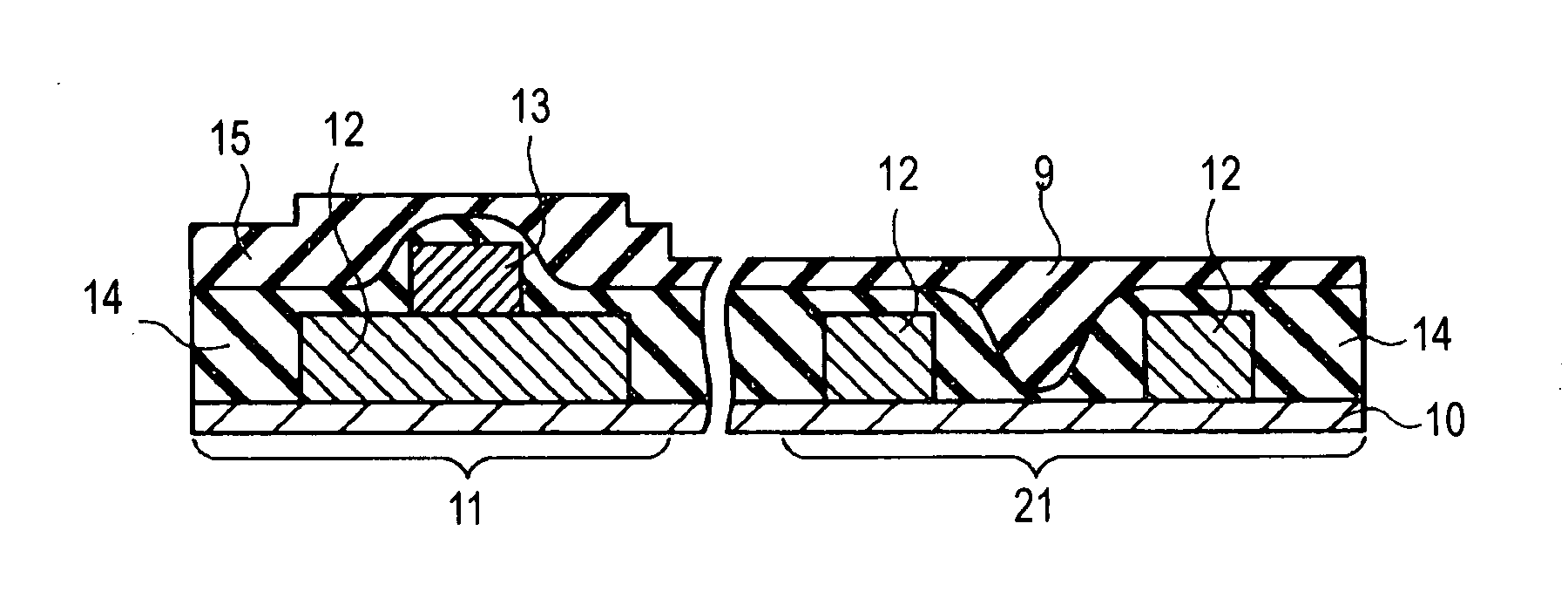
[0019]FIGS. 1A to 1D and 2A to 2C are sectional views for explaining a procedure according to a method of manufacturing a semiconductor device in accordance with the invention. In the following embodiment, description will be given by taking a solid-state image pick-up device as an example of a semiconductor device. The semiconductor device is not restricted to the solid-state image pick-up device but can also be applied to a CMOS type image sensor, for example

[0020] The solid-state image pick-up device according to the embodiment has a semiconductor substrate 10 constituted by silicon on which an impurity region is formed by ion doping, and the semiconductor substrate 10 is provided with a photoelectric converting portion such as a photodiode which is not shown and an electric charge transfer region for transferring an electric charge generated in the photoelectric converting portion.

[0021] The semiconductor substrate 10 has a peripheral circuit portion 11 to be a region in which ...

second embodiment

[0033] Next, description will be given to a second embodiment according to the invention. In the embodiment which will be described below, members having the same structures and functions as the members described above have the same designations or corresponding designations in the drawings, and description will be thus simplified or omitted.

[0034]FIGS. 3A to 3C are sectional views for explaining a procedure according to the second embodiment of the method of manufacturing a semiconductor device in accordance with the invention. In the embodiment, since a procedure for forming an insulating film 14 and a lens material layer 15 on a peripheral circuit portion 11 and a pixel portion 21 in a semiconductor substrate 10 is the same as that in the embodiment, description will be omitted.

[0035] As shown in FIG. 3A, a positive resist layer 27 for etching back the lens material layer 15 is formed in a thickness of 800 nm to 2400 nm on the lens material layer 15. In the related art, a thickn...


PUM


Abstract

A method of manufacturing a semiconductor device, the semiconductor device comprising: a semiconductor substrate; a pixel portion including an in-layer lens; and a peripheral circuit portion including a metal wiring portion, the pixel portion and the peripheral circuit portion being on the semiconductor substrate, the method comprising: forming an insulating film in the pixel portion and the peripheral circuit portion, so as to cover the metal wiring portion; providing, on the insulating film, a lens material layer for forming the in-layer lens; forming a resist layer for etching the lens material layer; curing the resist layer; and forming a first region and a second region in the resist layer, wherein a portion of the resist layer in the first region is thicker than that of the resist layer in the second region, the first region being in the peripheral circuit portion and the second region being in the pixel portion.

Description

BACKGROUND OF THE INVENTION [0001] 1. Field of the Invention [0002] The present invention relates to a method of manufacturing a semiconductor device, and more specifically, to a method of manufacturing a semiconductor device including an in-layer lens in a pixel portion. [0003] 2. Description of the Related Art [0004] As a semiconductor device, for example, there has been known a solid-state image pick-up device such as a CCD described in JP-A-2002-246578 and JP-A-2003-7988, for example. In the solid-state image pick-up device, a pixel portion of a semiconductor substrate includes a photoelectric converting portion such as a photodiode and an electric charge transfer portion for transferring an electric charge generated in the photoelectric converting portion, and a microlens is formed on a surface of the pixel portion. Moreover, some solid-state image pick-up devices have such a structure that a predetermined film (for example, a passivation film) in a layer of the pixel portion i...

Claims


Application Information

Patent Timeline
IPC IPC(8): H01L31/0232
CPCH01L27/14603H01L31/0232H01L27/14685H01L27/14625
Inventor YOSHIDA, TAKEO
Owner FUJIFILM CORP
Why Eureka
Try Eureka