Non-volatile flash memory structure and method for operating the same
- Summary
- Abstract
- Description
- Claims
- Application Information
AI Technical Summary
Benefits of technology
Problems solved by technology
Method used
Image
Examples
Embodiment Construction
[0015] The present invention solves the problems of multiple manufacturing steps, high degree of difficulty in fabrication and high production cost derived from complicated peripheral circuit design required by a higher operation current when fabricating a prior art non-volatile memory structure. The present invention also solves the problems of over erase and slow erase speed of memory structures of this type during the erase operation.
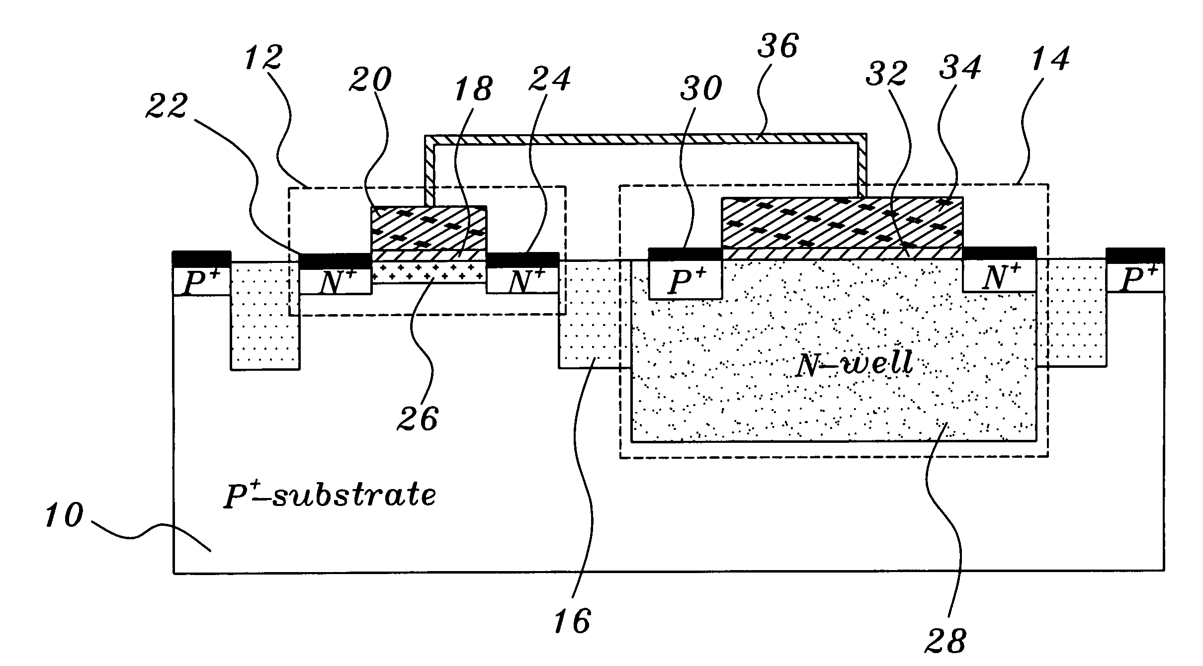
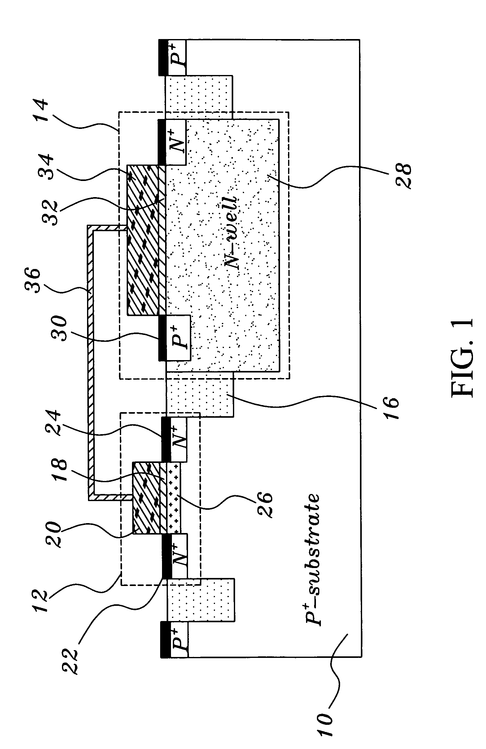
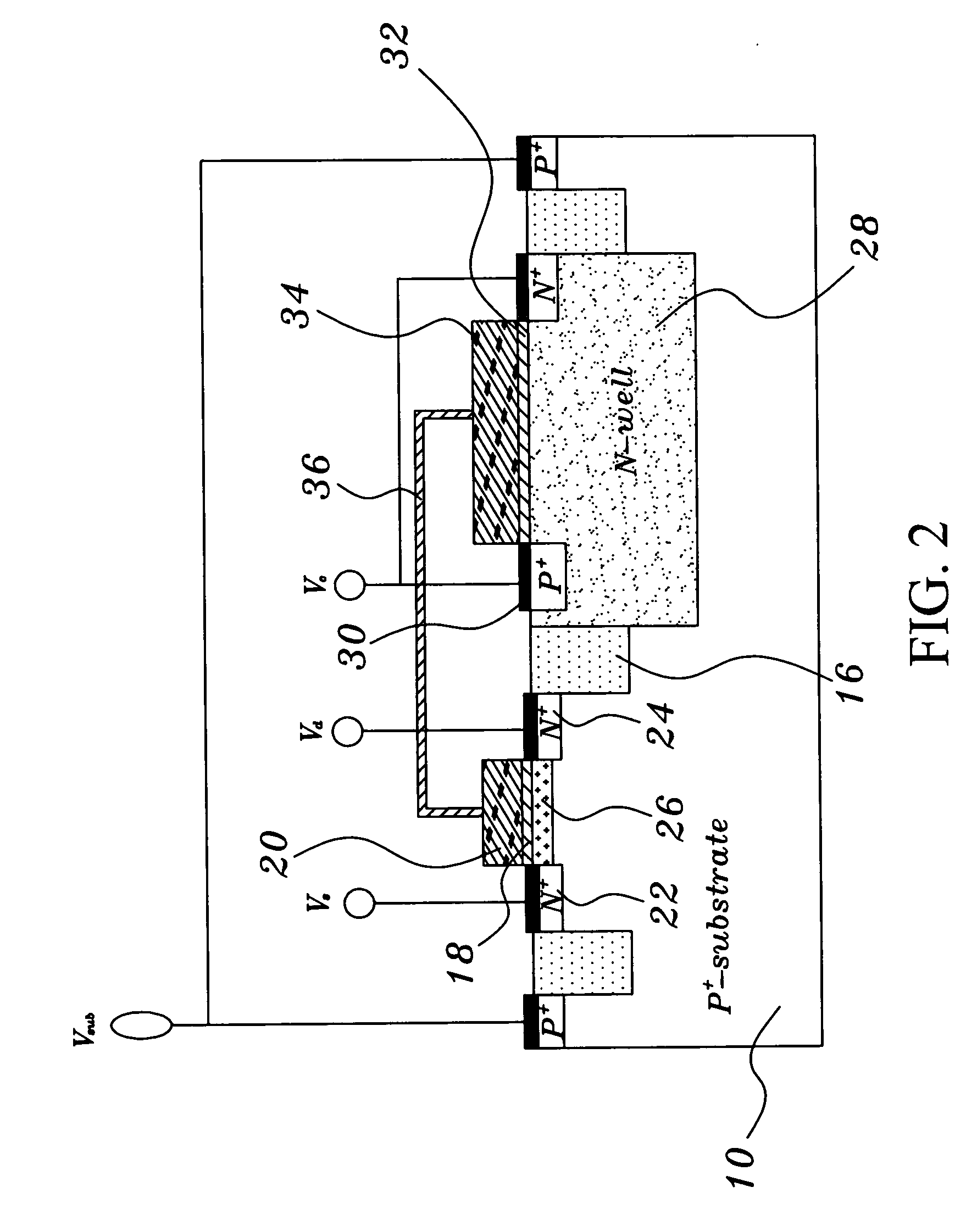
[0016] As shown in FIG. 1, a non-volatile memory structure comprises a p-type semiconductor substrate 10. A transistor structure 12 and a capacitor structure 14 that are isolated from each other are disposed on the semiconductor substrate 10. The transistor structure 12 and the capacitor structure 14 are isolated during the standard isolation process. This isolation process utilizes an isolator 16 to isolate the transistor structure 12 from the capacitor structure 14.
[0017] This transistor structure 12 is a MOSFET structure. This transistor structu...
PUM
 Abstract
Description
Claims
Application Information
 - R&D
- Intellectual Property
- Life Sciences
- Materials
- Tech Scout
- Unparalleled Data Quality
- Higher Quality Content
- 60% Fewer Hallucinations
Browse by: Latest US Patents, China's latest patents, Technical Efficacy Thesaurus, Application Domain, Technology Topic, Popular Technical Reports.
© 2025 PatSnap. All rights reserved.Legal|Privacy policy|Modern Slavery Act Transparency Statement|Sitemap|About US| Contact US: help@patsnap.com


