Efficient white-light OLED display with filters
a filter and white light technology, applied in the direction of discharge tube luminescnet screens, discharge tube/lamp details, electric discharge lamps, etc., can solve the problems of difficult to achieve light emission with strong intensity, three-layer structure shows diminished efficiency, and manufacturing difficulties, so as to improve power efficiency, improve color gamut, and reduce voltage requirements
- Summary
- Abstract
- Description
- Claims
- Application Information
AI Technical Summary
Benefits of technology
Problems solved by technology
Method used
Image
Examples
example 1
Comparative Two-Layer
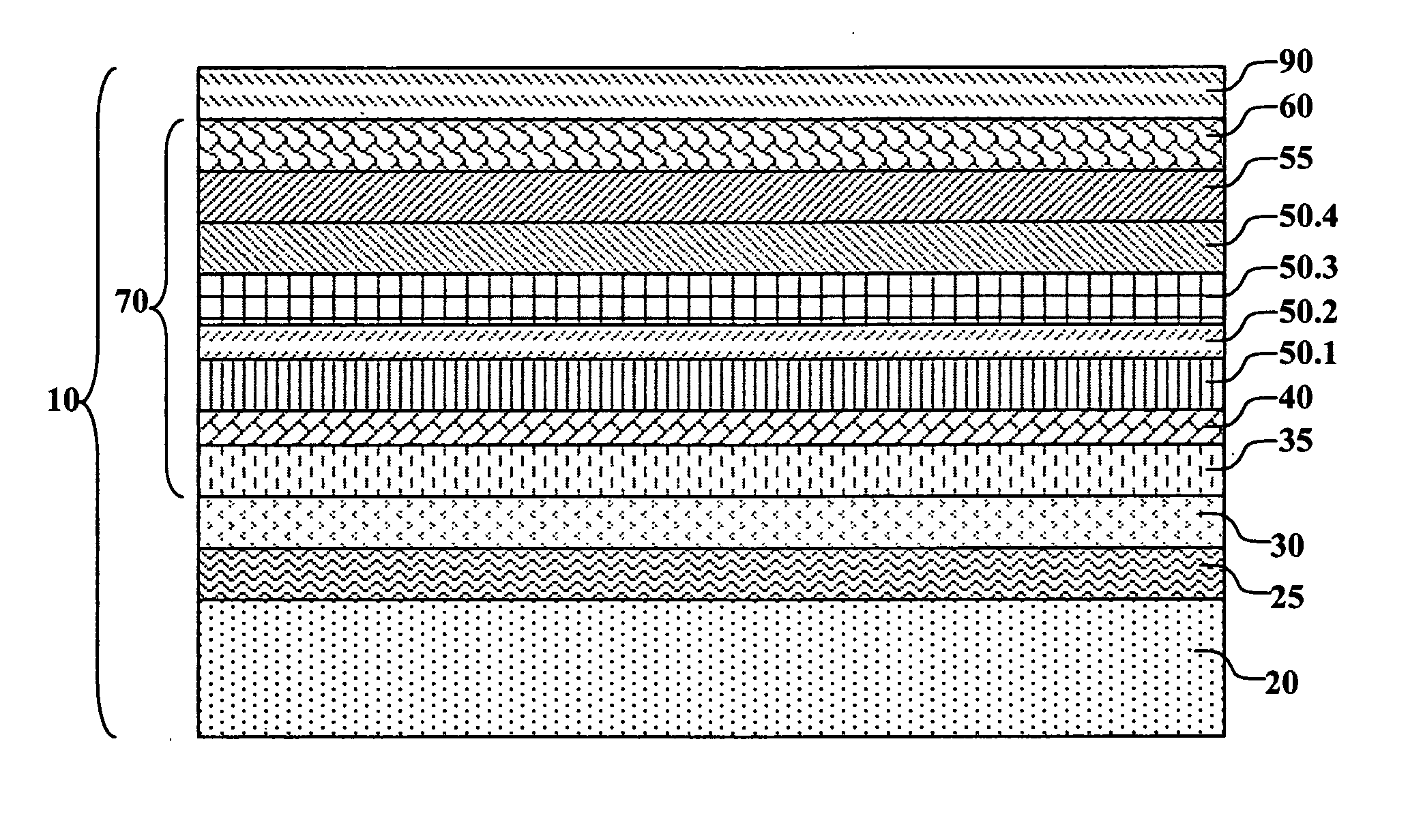
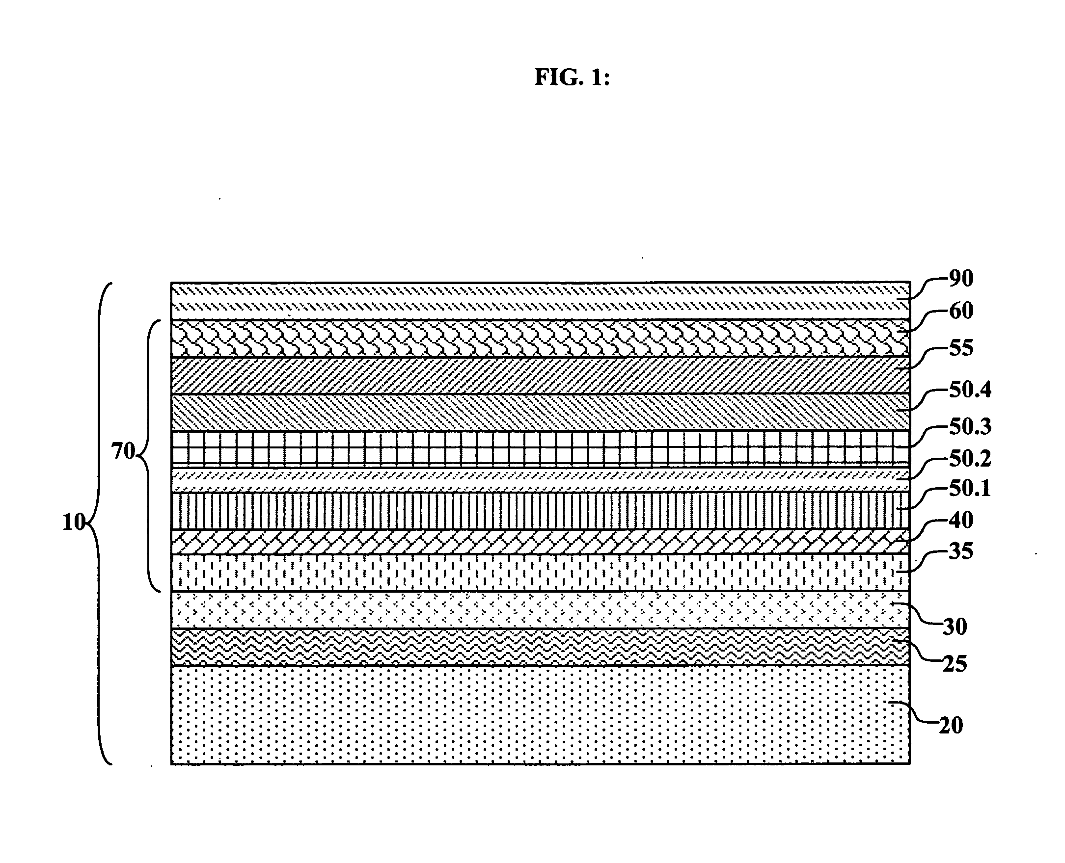
[0101] A comparative color OLED display was constructed in the following manner: [0102] 1. A clean glass substrate was deposited by sputtering with indium tin oxide (ITO) to form a transparent electrode of 85 nm thickness. [0103] 2. The above-prepared ITO surface was treated with a plasma oxygen etch. [0104] 3. The above-prepared substrate was further treated by vacuum-depositing a 10 nm layer of hexacyanohexaazatriphenylene (CHATP) as a hole-injecting layer (HIL). [0105] 4. The above-prepared substrate was further treated by vacuum-depositing a 10 nm layer of 4,4′-bis[N-(1-naphthyl)-N-phenylamino]biphenyl (NPB) as a hole-transporting layer (HTL). [0106] 5. The above-prepared substrate was further treated by vacuum-depositing a 20 nm yellow light-emitting layer including 14 nm NPB (as host) and 6 nm 9,10-bis(2-naphthyl)anthracene (ADN) as a stabilizer with 2% yellow-orange emitting dopant diphenyltetra-t-butylrubrene (PTBR). [0107] 6. The above-prepared subst...
example 2
Comparative Three-Layer
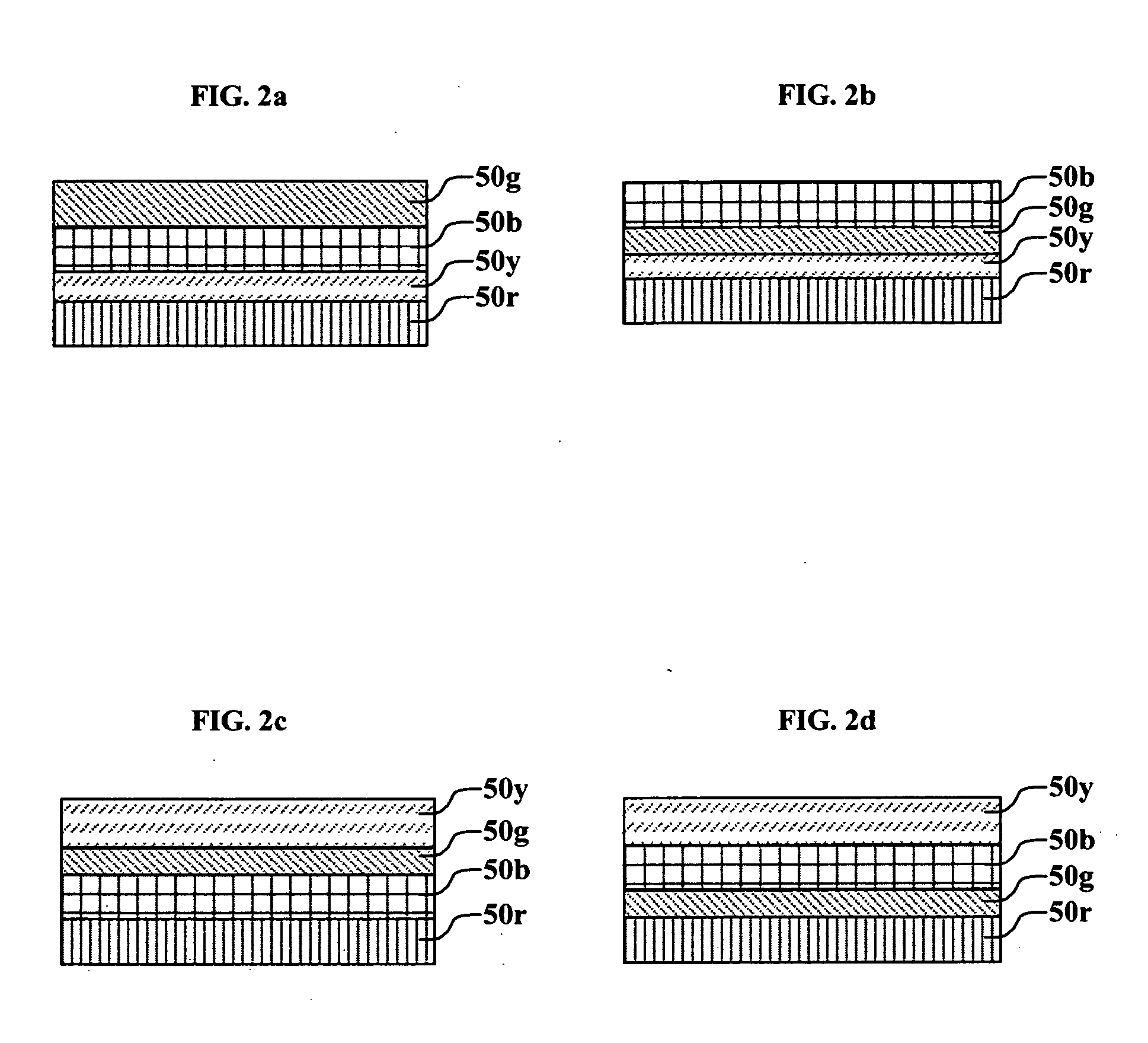
[0110] A comparative color OLED display was constructed in the following manner: [0111] 1. A clean glass substrate was deposited by sputtering with ITO to form a transparent electrode of 60 nm thickness. [0112] 2. The above-prepared ITO surface was treated with a plasma oxygen etch. [0113] 3. The above-prepared substrate was further treated by vacuum-depositing a 10 nm layer of CHATP as a hole-injecting layer (HIL). [0114] 4. The above-prepared substrate was further treated by vacuum-depositing a 10 nm layer of NPB as a hole-transporting layer (HTL). [0115] 5. The above-prepared substrate was further treated by vacuum-depositing a 20 nm red light-emitting layer including 14 nm of NPB and 6 nm BNA as a stabilizer doped with 0.5% dibenzo {[f,f′]-4,4′7,7′-tetraphenyl]diindeno-[1,2,3-cd:1′,2′,3′-lm]perylene (TPDBP) as a red emitting dopant. [0116] 6. The above-prepared substrate was further treated by vacuum-depositing a 15 nm blue light-emitting layer including ...
example 3
Inventive
[0120] An inventive color OLED display was constructed in the following manner: [0121] 1. A clean glass substrate was deposited by sputtering with ITO to form a transparent electrode of 60 nm thickness. [0122] 2. The above-prepared ITO surface was treated with a plasma oxygen etch. [0123] 3. The above-prepared substrate was further treated by vacuum-depositing a 10 nm layer of CHATP as a hole-injecting layer (HIL). [0124] 4. The above-prepared substrate was further treated by vacuum-depositing a 10 nm layer of NPB as a hole-transporting layer (HTL). [0125] 5. The above-prepared substrate was further treated by vacuum-depositing a 18 nm red light-emitting layer including 12.6 nm of NPB and 5.4 nm BNA as a stabilizer doped with 0.5% TPDBP as a red emitting dopant. [0126] 6. The above-prepared substrate was further treated by vacuum-depositing a 2 nm yellow light-emitting layer including 1.4 nm NPB (as host) and 0.6 nm ADN as a stabilizer with 3% yellow-orange emitting dopant...
PUM
 Abstract
Description
Claims
Application Information
 - R&D
- Intellectual Property
- Life Sciences
- Materials
- Tech Scout
- Unparalleled Data Quality
- Higher Quality Content
- 60% Fewer Hallucinations
Browse by: Latest US Patents, China's latest patents, Technical Efficacy Thesaurus, Application Domain, Technology Topic, Popular Technical Reports.
© 2025 PatSnap. All rights reserved.Legal|Privacy policy|Modern Slavery Act Transparency Statement|Sitemap|About US| Contact US: help@patsnap.com


