
Liquid crystal display panel, display device, and manufacturing method of liquid crystal display panel

A technology for a liquid crystal display panel and a manufacturing method, which is applied to instruments, nonlinear optics, optics, etc., can solve the problems of insufficiently vivid and true colors, decreased aperture ratio, large equipment deviation, etc., to improve display quality, improve brightness, increase The effect of opening ratio

Active Publication Date: 2013-07-31
BEIJING BOE OPTOELECTRONCIS TECH CO LTD
View PDF10 Cites 42 Cited by
  • Summary
  • Abstract
  • Description
  • Claims
  • Application Information

AI Technical Summary

Problems solved by technology

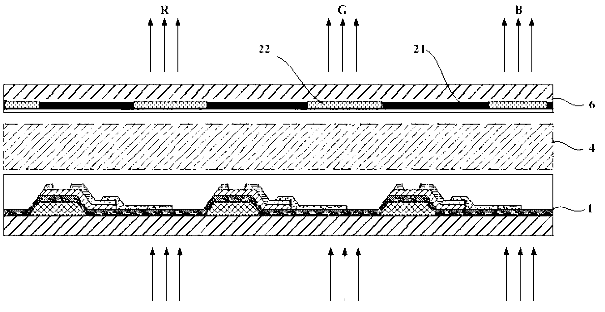
[0005] like figure 1 As shown, the existing liquid crystal display panel includes the array substrate 1 and the color filter substrate 6 of the box, and the liquid crystal layer 4 located between the array substrate 1 and the color filter substrate 6, and the backlight used in the existing liquid crystal display panel It is a white backlight, the white backlight is mixed light with blue light and yellow light, and the color is not pure, the white backlight is filtered by the red, green and blue primary colors (R\G\B) of the color filter layer 22 in the color film substrate 6 The obtained monochromatic light contains a variety of colors that are not expected, which leads to a relatively low color gamut of the picture, and the colors are not vivid enough; in addition, when the array substrate 1 and the color filter substrate 6 are aligned, the equipment deviation is large, so it is necessary to The black matrix 21 is made wider, but this leads to a decrease in the aperture ratio

Method used


Image

  • Liquid crystal display panel, display device, and manufacturing method of liquid crystal display panel
  • Liquid crystal display panel, display device, and manufacturing method of liquid crystal display panel
  • Liquid crystal display panel, display device, and manufacturing method of liquid crystal display panel

Examples


Embodiment Construction

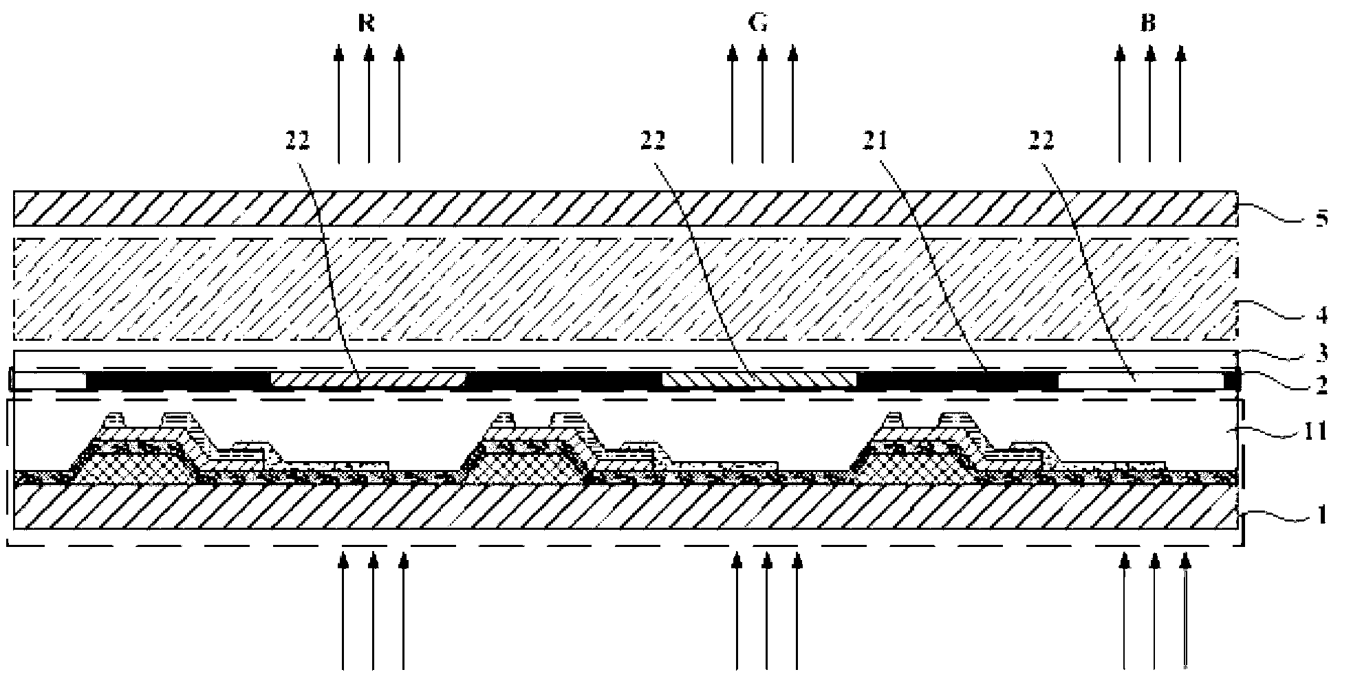
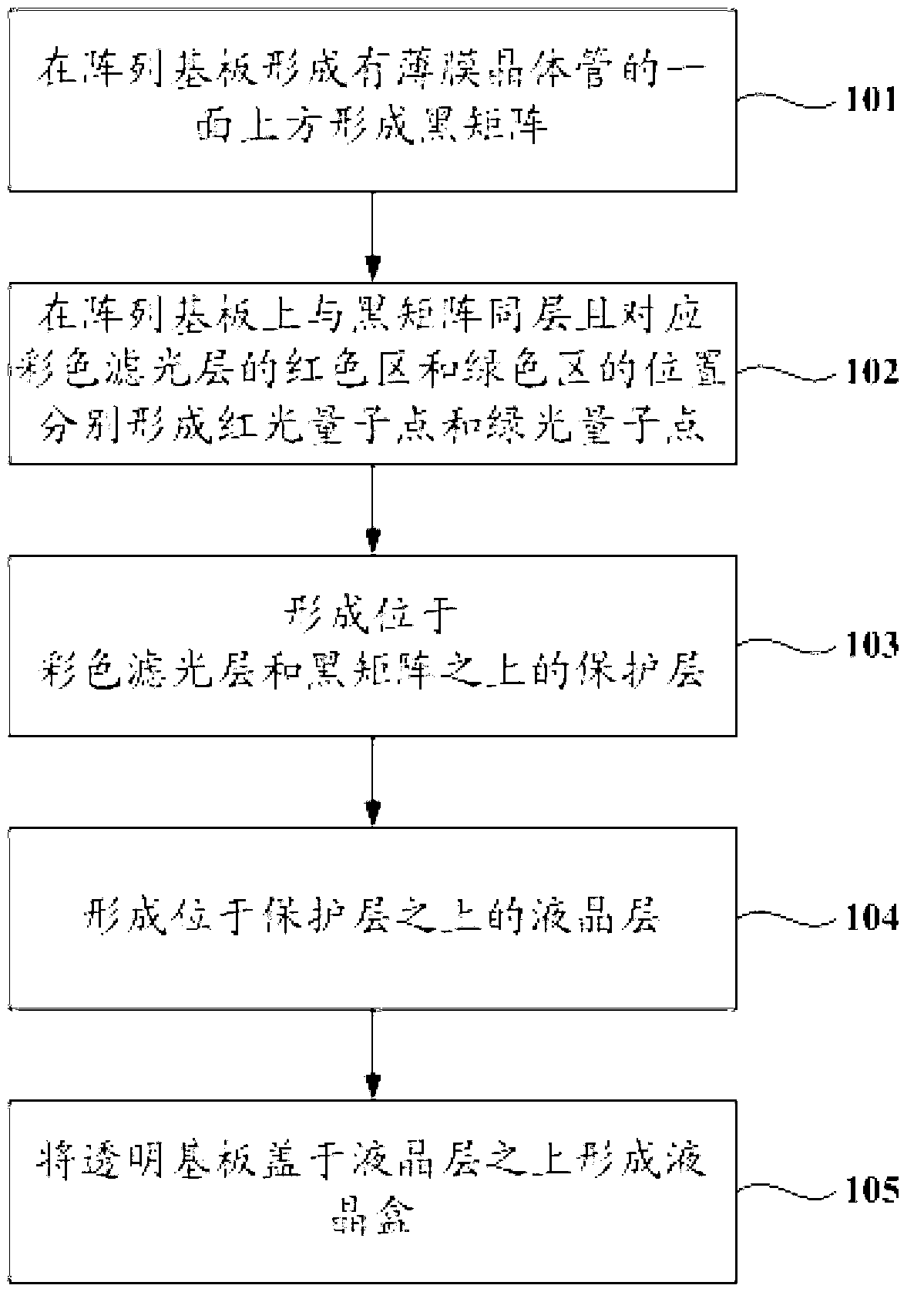
[0044] In order to improve the color gamut of the picture, the invention provides a liquid crystal display panel, a display device and a manufacturing method of the liquid crystal display panel. The liquid crystal display panel includes an array substrate, and further includes: a color filter located on the array substrate, the color filter includes a black matrix and a color filter layer with different color regions, wherein the Different color regions of the color filter layer have quantum dots of different sizes, and the quantum dots of different sizes generate corresponding colors through excitation; a protective layer located on the color filter; located on the protective layer a liquid crystal layer; a transparent protective plate located on the liquid crystal layer.

[0045] In this technical solution, due to the use of quantum dots that can generate different monochromatic lights through excitation, the emission spectrum of quantum dots is narrow and the luminous effic...


PUM

PropertyMeasurementUnit
particle diameteraaaaaaaaaa
sizeaaaaaaaaaa
sizeaaaaaaaaaa

Abstract

The invention relates to the technical field of liquid crystal display and discloses a liquid crystal display panel, a display device, and a manufacturing method of the liquid crystal display panel. The liquid crystal display panel comprises a color filter, a protective layer, a liquid crystal layer and a transparent protective plate, wherein the color filter is positioned on an array substrate and comprises a black matrix and a color filter layer with different color regions; the different color regions respectively have different sizes of quantum dots; the different sizes of quantum dots generate corresponding colors through excitation; the protective layer is positioned on the liquid crystal layer; the liquid crystal layer is positioned on the protective layer; and the transparent protective plate is positioned on the liquid crystal layer. According to the technical scheme of the invention, the emission spectrum of the quantum dots is narrow and the luminous efficiency is high, and light of backlight can be efficiently converted into light closed to monochromatic light, so the color gamut of the liquid crystal display panel is greatly improved and the display quality of the display panel is improved.

Description

technical field [0001] The invention relates to the technical field of liquid crystal display, in particular to a liquid crystal display panel, a display device and a manufacturing method of the liquid crystal display panel. Background technique [0002] Semiconductor quantum dots (Quantum Dots, QDs), also known as nanocrystals, are aggregates of a limited number of nanoscale atoms and molecules, generally with a particle size ranging from 2-20nm. At present, there are mainly group IV, III-V and II-VI quantum dot materials. Among them, II-VI quantum dot materials are widely used because of their easy preparation and excitation spectrum almost covering visible light. [0003] When the particle size of nanomaterials drops to a certain value (generally below 10nm), the electronic energy level near the metal Fermi level changes from quasi-continuous to discrete energy levels, and the discontinuous highest occupied molecular orbitals and The energy gap of the lowest unoccupied ...

Claims


Application Information

Patent Timeline
Patent Type & Authority Applications(China)
IPC IPC(8): G02F1/1335G02F1/1333
CPCG02F1/133617G02F2202/36G02F1/133514G02F1/133516G02F1/133512G02F1/133603G02F1/133609
Inventor 董瑞君孙海威董学
Owner BEIJING BOE OPTOELECTRONCIS TECH CO LTD
Learn More