Gas-barrier film, substrate film, and organic electroluminescent device
a substrate film and gas-barrier technology, applied in the direction of discharge tube luminescnet screens, superimposed coating processes, natural mineral layered products, etc., can solve the problems of degraded parts, degraded parts may be a display failure, and poor gas-barrier properties, etc., to achieve high producibility, high durability and flexible
- Summary
- Abstract
- Description
- Claims
- Application Information
AI Technical Summary
Benefits of technology
Problems solved by technology
Method used
Image
Examples
example 1
[0144]Gas-barrier films (samples Nos. 1 to 20), comprising a gas-barrier laminate formed on a substrate film and a transparent conductive layer formed on the laminate, were fabricated according to the process mentioned below. The details of the structure of each gas-barrier film are shown in Table 1 and Table 2.
Fabrication of Gas-Barrier Films of the Invention (Samples Nos. 1 to 11):
1. Formation of Substrate Film:
[0145]A substrate film of a resin shown in Table 1, having a thickness of 100 μm, was prepared. In Table 1, PET is Toray's Lumilar T60; and PEN is Teijin-DuPont Film's Teonex Q65FA.
2. Formation of Gas-Barrier Laminate:
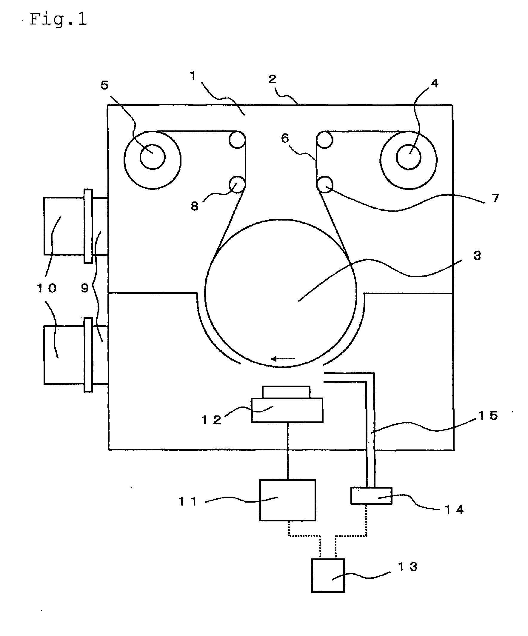
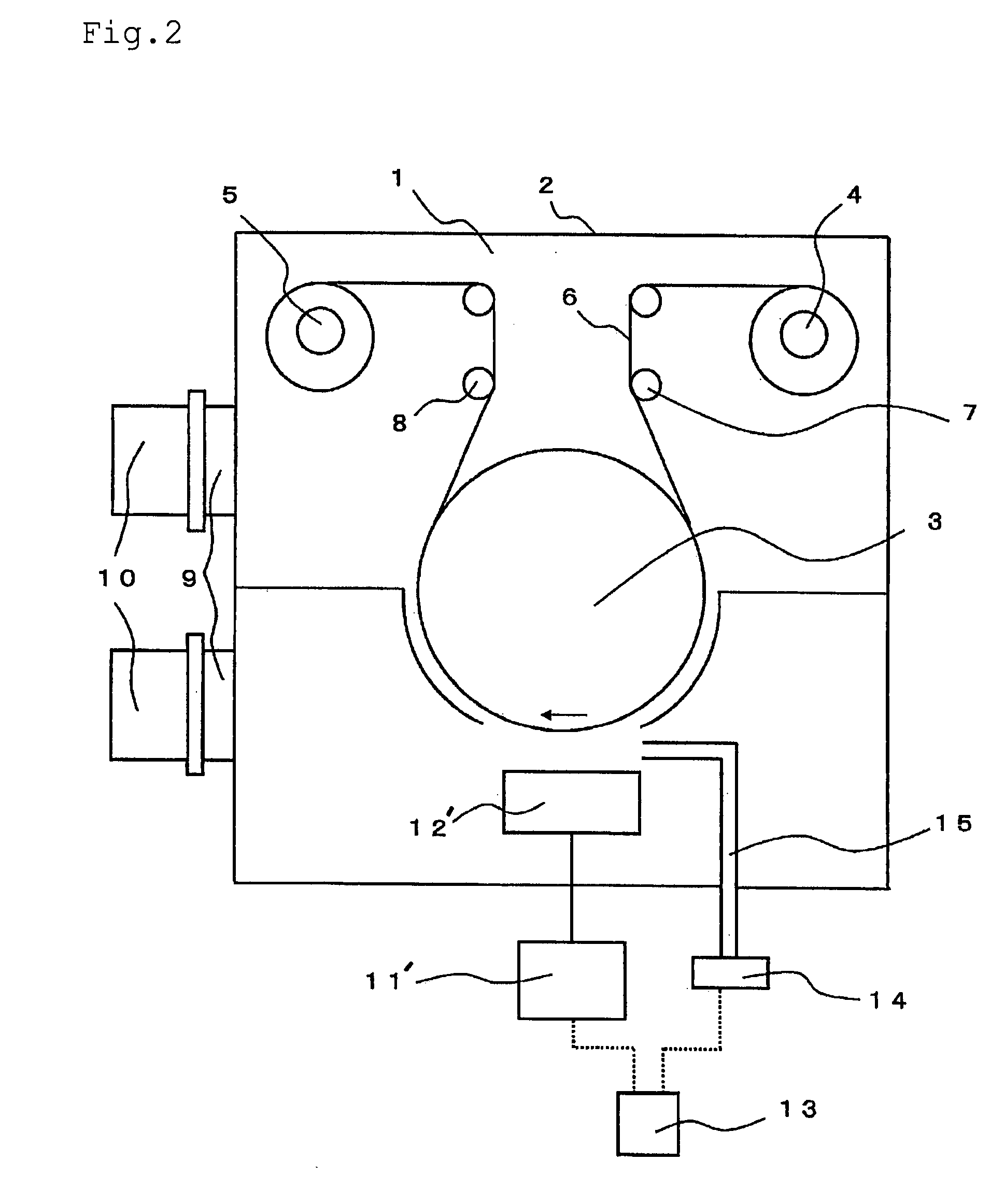
[0146]Using a roll-to-roll inductively-coupled plasma CVD device (1) shown in FIG. 1, an inorganic gas-barrier layer was formed on a substrate film. As in FIG. 1, the inductively-coupled plasma CVD device (1) has a vacuum chamber (2); and in the center part thereof, a drum (3) is disposed to cool a plastic film (6) that is kept in contact with its surface. In ...
example 2
Fabrication of Organic EL Device (I):
[0174]On the above-mentioned, transparent conductive layer-coated gas-barrier film (samples Nos. 1 to 20) having a size of 25 mm×25 mm, formed was an indium tin oxide (ITO, indium / tin=95 / 5 by mol) anode (thickness 0.2 μm) according to a sputtering method and using a direct current source. On the anode, formed was a hole injection layer of copper phthalocyanine (CuPc, 10 nm) according to a vacuum evaporation method; and a hole transportation layer of N,N′-dinaphthyl-N,N′-diphenylbenzidine (40 nm) was formed on it according to a vacuum evaporation method. With that, a host material of 4,4′-N,N′-dicarbazole-biphenyl, a blue-emitting material of bis[4,6-difluorophenyl)-pyridinato-N,C2′](picolinate)iridium complex (Firpic), a green-emitting material of tris(2-phenylpyridine)iridium complex (Ir(ppy)3), and a red-emitting material of bis(2-phenylquinoline)acetylacetonato / iridium were co-deposited on it, in a ratio of 100 / 2 / 4 / 2 by mass, thereby forming a...
PUM
| Property | Measurement | Unit |
|---|---|---|
| glass transition temperature | aaaaa | aaaaa |
| refractive index | aaaaa | aaaaa |
| thickness | aaaaa | aaaaa |
Abstract
Description
Claims
Application Information
 - R&D
- Intellectual Property
- Life Sciences
- Materials
- Tech Scout
- Unparalleled Data Quality
- Higher Quality Content
- 60% Fewer Hallucinations
Browse by: Latest US Patents, China's latest patents, Technical Efficacy Thesaurus, Application Domain, Technology Topic, Popular Technical Reports.
© 2025 PatSnap. All rights reserved.Legal|Privacy policy|Modern Slavery Act Transparency Statement|Sitemap|About US| Contact US: help@patsnap.com


