A method for fabricating a capacitor structure

Active Publication Date: 2007-09-20
UNITED MICROELECTRONICS CORP
View PDF18 Cites 8 Cited by
  • Summary
  • Abstract
  • Description
  • Claims
  • Application Information

AI Technical Summary

Benefits of technology

[0021] Accordingly, the first metal layer in the substrate and the connection layer, which is disposed on a portion of the first metal layer, the sidewall of the opening and a portion of the etching stop layer, together form a lower electrode of the capacitor. Since the formation of the first metal layer can be integrated with that of a level of interconnect structure and the definition of the opening in the etching stop layer can be integrated with the forming process of alignment marks, only one extra photomask is required in the capacitor fabrication for sequentially defining the second metal layer, the insulating layer and the connection layer. Accordingly, the method of this invention can save one photomask as compared with the prior art.

Problems solved by technology

Since the space for forming capacitors are also much reduced correspondingly, the capacitors have insufficient capacitance.
This problem is particularly significant in deep sub-micron processes.
MIM capacitors and MOM capacitors are widely used in deep sub-micron IC products, but adversely have lower unit-area capacitance.
A method to increase the capacitance is to decrease the thickness of the dielectric film between the electrodes, but the uniformity and stability of a thin dielectric film is difficult to control.
Another method is to form 3D electrodes with larger surface areas, but the forming process is quite complicated making the mass production difficult.
Still another method is to use a high-k material to achieve higher unit-area capacitance, but the reliability of such a capacitor is often insufficient.
However, because the forming processes of the upper electrode 108a and the lower electrode 104a cannot be integrated with other semiconductor processes, two extra photomasks are needed making the above method complicated and costly.

Method used


Image

  • A method for fabricating a capacitor structure
  • A method for fabricating a capacitor structure
  • A method for fabricating a capacitor structure

Examples


Embodiment Construction

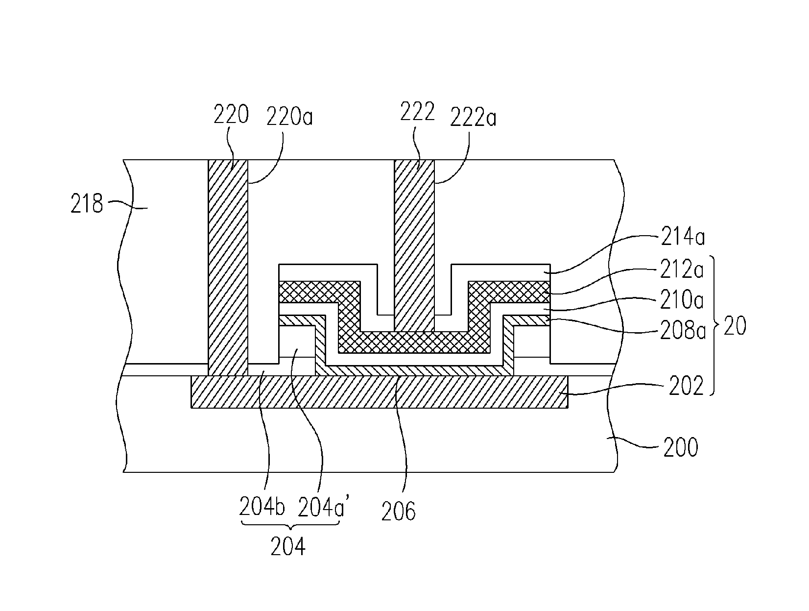
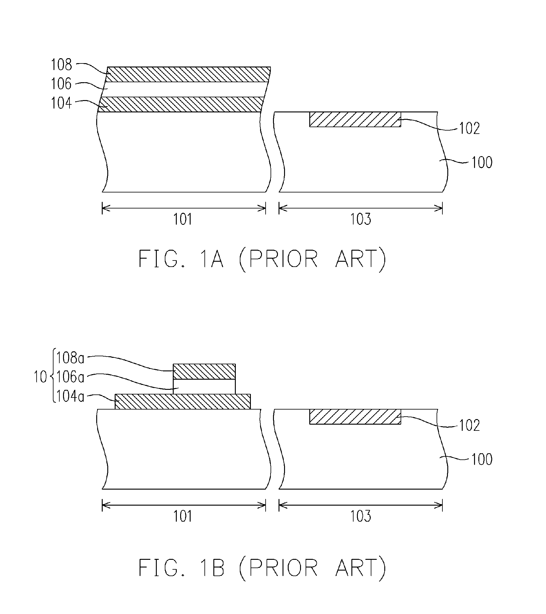
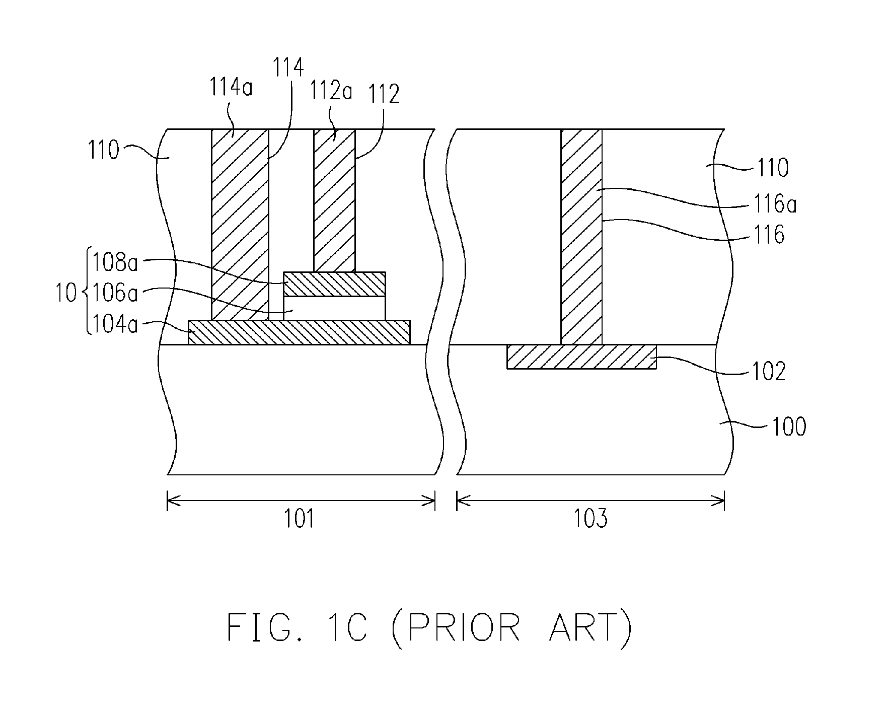
[0027] Referring to FIG. 2A, a substrate 200 is provided, having a metal layer 202 and semiconductor devices (not shown) therein, wherein the metal layer 202 is a part of the lower electrode of the capacitor of this embodiment, as explained later. The material of the metal layer 202 may be copper (Cu). An etching stop layer, such as a composite layer of a SiN layer 204b and a SiO layer 204a thereon, is formed on the substrate 200, possibly through CVD. In other embodiments, the etching stop layer 204 may alternatively be a single SiO or SiN layer. Then, an opening 206 is formed in the etching stop layer 204 exposing a portion of the metal layer 202. The opening 206 may be formed by forming a patterned photoresist layer over the substrate 200 exposing the corresponding portion of the etching stop layer 204, etching the etching stop layer 204 with the photoresist layer as a mask and then removing the photoresist layer. It is particularly noted that the metal layer 202 can be defined s...


PUM


Abstract

A capacitor structure is described, including a substrate, a first metal layer in the substrate, an etching stop layer on the substrate having therein an opening that exposes a portion of the first metal layer, a connection layer on the portion of the first metal layer, the sidewall of the opening and a portion of the etching stop layer, a second metal layer over the connection layer, and an insulating layer between the second metal layer and the connection layer.

Description

BACKGROUND OF THE INVENTION [0001] 1. Field of the Invention [0002] The present invention relates to a structure of an IC device and fabrication of the same. More particularly, the present invention relates to a capacitor structure and a method for fabricating the same. [0003] 2. Description of the Related Art [0004] As the integration degree of semiconductor devices is greatly increased, the sizes of the same are much reduced. Since the space for forming capacitors are also much reduced correspondingly, the capacitors have insufficient capacitance. This problem is particularly significant in deep sub-micron processes. [0005] There are three categories of capacitors in general, including metal-insulator-metal (MIM) capacitor, metal-line to metal-line (MOM) capacitor and metal-insulator-silicon (MIS) capacitor. MIM capacitors and MOM capacitors are widely used in deep sub-micron IC products, but adversely have lower unit-area capacitance. [0006] A method to increase the capacitance i...

Claims


Application Information

Patent Timeline
IPC IPC(8): H01L23/48H01L23/52H01L29/40
CPCH01L23/5223H01L2924/0002H01L2924/00
Inventor TSAI, MINGSHANG
Owner UNITED MICROELECTRONICS CORP
Why Eureka
Try Eureka