
Thin silicon or germanium sheets and photovoltaics formed from thin sheets

Inactive Publication Date: 2007-09-13
NANOGRAM
View PDF44 Cites 84 Cited by
  • Summary
  • Abstract
  • Description
  • Claims
  • Application Information

AI Technical Summary

Benefits of technology

[0011]In additional aspects, the invention relates to a display comprising a control element and a plurality of light emitting elements with light emission of each element being under the control of the control elemen...

Problems solved by technology

With increasing costs and undesirable environmental effects from the use of fossil fuels and other non-renewable energy sources, there are growing demands for alternative forms of energy.

Method used

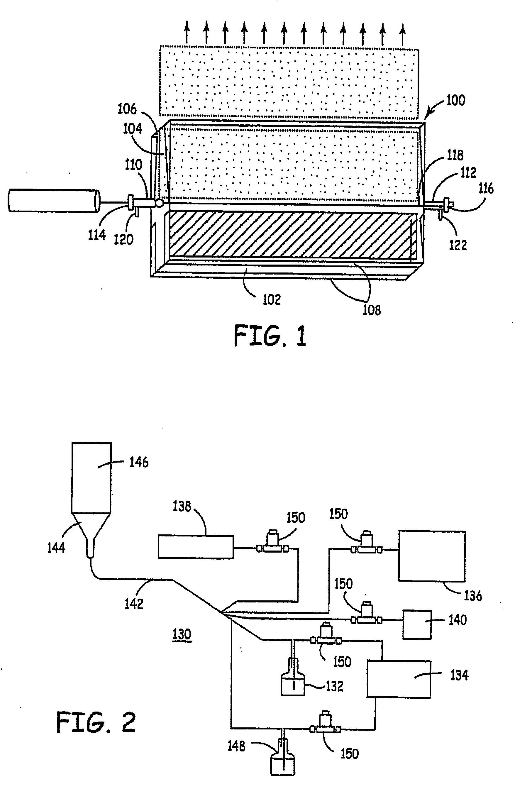

Image

  • Thin silicon or germanium sheets and photovoltaics formed from thin sheets
  • Thin silicon or germanium sheets and photovoltaics formed from thin sheets
  • Thin silicon or germanium sheets and photovoltaics formed from thin sheets

Examples


example

[0258]In this example, the formation of a relatively dense silicon sheet over a release layer is described.

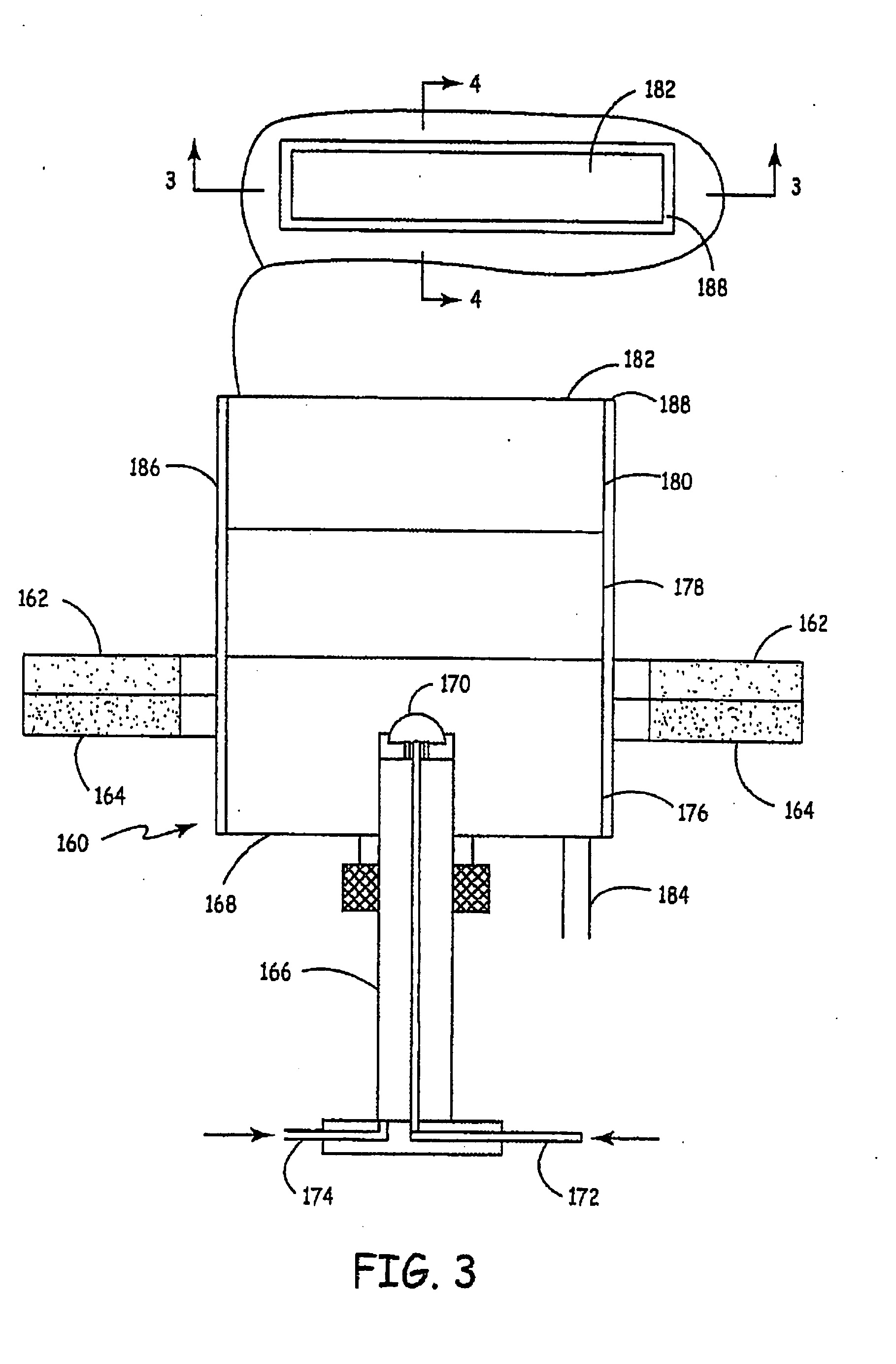
[0259]These experiments were performed on an apparatus similar to the apparatus shown in FIGS. 8-10 having a configuration with reactants delivered from the top of the reaction chamber. With respect to the particular apparatus used for the experiments, a cut-away view of reaction chamber 700 showing a stage 702 mounted below the reactant inlet nozzle 704 is shown in FIG. 27. Stage 702 is adjustable such that the distance from the substrate to the center of the light beam can be adjusted between 1 mm to 20 mm. The light beam can enter chamber 700 through opening 706 in mount 708 on light tube 710. An exit light tube 712 receives the beam after transmission through the chamber. Stage 702 connects to an actuator arm that enters chamber 700 through actuator port 714.

[0260]A separate view of stage 702 is shown in FIG. 28. Stage 702 comprises a stainless steal support platform 720 wi...


PUM

PropertyMeasurementUnit
Thicknessaaaaaaaaaa
Thicknessaaaaaaaaaa
Thicknessaaaaaaaaaa

Abstract

Thin semiconductor foils can be formed using light reactive deposition. These foils can have an average thickness of less than 100 microns. In some embodiments, the semiconductor foils can have a large surface area, such as greater than about 900 square centimeters. The foil can be free standing or releasably held on one surface. The semiconductor foil can comprise elemental silicon, elemental germanium, silicon carbide, doped forms thereof, alloys thereof or mixtures thereof. The foils can be formed using a release layer that can release the foil after its deposition. The foils can be patterned, cut and processed in other ways for the formation of devices. Suitable devices that can be formed form the foils include, for example, photovoltaic modules and display control circuits.

Description

CROSS REFERENCE TO RELATED APPLICATIONS[0001]The application claims priority to copending U.S. Provisional Patent Application Ser. No. 60 / 782,115, filed on Mar. 13, 2006 to Hieslmair et al., entitled “Thin Silicon or Germanium Sheets and Photovoltaics Formed From Thin Sheets,” incorporated herein by reference.FIELD OF THE INVENTION[0002]The invention relates to thin sheets, which may be free standing, of elemental silicon, elemental germanium, alloys thereof, silicon carbide or doped materials thereof having a large surface area. The invention further relates to methods for forming free standing sheets with large surface areas. The invention also relates to structures incorporating thin sheets of elemental silicon, elemental germanium, alloys thereof, silicon carbide or doped materials thereof and in particular photovoltaic cells and display controllers.BACKGROUND OF THE INVENTION[0003]Crystalline silicon is extensively used in the production of integrated circuits. For these applic...

Claims


Application Information

Patent Timeline
IPC IPC(8): B32B33/00
CPCC23C16/01Y10T428/14C23C16/482C23C16/483C23C16/54H01L31/0236H01L31/035281H01L31/03682H01L31/068H01L31/18H01L31/1804H01L31/1812H01L31/182Y02E10/546Y02E10/547H01L31/0475Y10T29/41Y10T428/24802C23C16/24Y02P70/50H01L21/20
Inventor HIESLMAIR, HENRYMOSSO, RONALD J.LYNCH, ROBERT B.CHIRUVOLU, SHIVKUMARMCGOVERN, WILLIAM E.HORNE, CRAIG R.SOLAYAPPAN, NARAYANCORNELL, RONALD M.
Owner NANOGRAM
Learn More