Thin film transistor and organic electroluminescent display device

a thin film transistor and display device technology, applied in the direction of electroluminescent light sources, thermoelectric devices, electric lighting sources, etc., can solve the problems of deteriorating display contrast, exacerbated display quality, and unstable characteristics of transistors, so as to reduce variations in characteristics (for example, a threshold voltage) and suppress photoelectric current generation

Inactive Publication Date: 2007-09-13
SANYO ELECTRIC CO LTD
View PDF12 Cites 43 Cited by
  • Summary
  • Abstract
  • Description
  • Claims
  • Application Information

AI Technical Summary

Benefits of technology

[0010] The light-shielding layer is formed to cover only the boundary region, considering that a primary region where a photoelectric current is generated by an influence of the extraneous light is the reverse biased boundary region between the drain region and the channel region. As a result, the generation of the photoelectric current can be suppressed and variations in characteristics (for example, a threshold voltage) of the thin film transistor can be reduced.

Problems solved by technology

There arises a problem that contrast of the display is deteriorated, since the extraneous light excites carriers in the active layer in the thin film transistor to cause a photoelectric current (leakage current) between a source and a drain of the thin film transistor.
If the electric potential at the light-shielding layer is not fixed, on the other hand, the electric potential at the light-shielding layer becomes unstable because of electrostatic charging, thereby causing a problem that the characteristics of the transistor become even more unstable.
When such a thin film transistor is used as the drive transistor in the organic EL display device, there arises a problem that quality of the display is exacerbated.

Method used


Image

  • Thin film transistor and organic electroluminescent display device
  • Thin film transistor and organic electroluminescent display device
  • Thin film transistor and organic electroluminescent display device

Examples


second embodiment

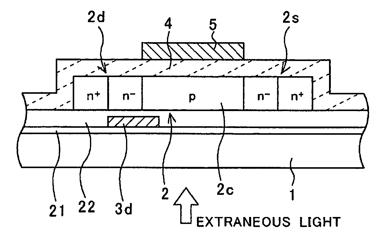
[0030] Considering the above, a thin film transistor according to this invention is provided with a second light-shielding layer 3s that covers only a boundary region between the source region 2s and the channel region 2c, in addition to the drain-light-shielding layer (a first light-shielding layer) 3d, as shown in FIG. 3. The insulating film 22 is also interposed between the second light-shielding layer 3s and the active layer 2.

[0031] This thin film transistor is effective to suppress the generation of the photoelectric current when the p-n junction associated with the drain region 2d is reverse biased and when the p-n junction associated with the source region 2s is also reverse biased. In addition, because it is not full-light-shielded, the variation in the characteristics due to the variation in the electric potential at the light-shielding layer 3d and the light-shielding layer 3s is suppressed to some extent.

[0032] Although the first and second embodiments are described for...

third embodiment

[0039]FIG. 7 is a circuit diagram of one of the pixels in the organic EL display device according to this invention. A pixel selection transistor T1 is shown in the circuit diagram, in addition to the drive transistor T2. The pixel selection transistor T1 is turned on in response to a gate signal on a gate line GL to transfer a video signal Vsig to the gate of the drive transistor T1. A storage capacitor Cs retains the video signal Vsig. The pixel selection transistor T1 is of n-channel type and the drive transistor T2 is of p-channel type.

[0040] When illuminated by extraneous light as intensive as 100,000 lux, a photoelectric current (off leakage current) is caused in the pixel selection transistor T1 to discharge the charges stored at the gate of the drive transistor T2. As a result, there is caused vertical interference among the pixels, that is, display failure due to crosstalk. In order to avoid it, the pixel selection transistor T1 also needs to be provided with a light-shield...

fifth embodiment

[0042]FIG. 9 shows a circuit diagram of one of pixels in an organic EL display device according to this invention. It is the most preferable circuit in which a drive transistor T2 is provided with a drain-light-shielding layer 3d while a pixel selection transistor T1 is provided with a drain-light-shielding layer 3d and a source-light-shielding layer 3s (Refer to FIG. 3.). As a result, the photoelectric current (off leakage current) caused by the extraneous light can be suppressed to improve the display contrast and the variation in the characteristics (the variation in the threshold voltage, for example) of the transistor can be reduced regardless the high level voltage of the gate signal and the video signal Vsig, for both the drive transistor T2 and the pixel selection transistor T1.

[0043] With the thin film transistors of these embodiments, the variation in the characteristics (threshold voltage, for example) of the thin film transistor can be reduced, while the photoelectric cu...


PUM


Abstract

A photoelectric current caused by extraneous light is suppressed and variations in characteristics (for example, a threshold voltage) of a thin film transistor are reduced. An active layer (semiconductor layer) made of polycrystalline silicon, which is transformed from amorphous silicon by laser annealing, is formed on an insulating substrate. A drain region 2d and a source region 2s, which are facing to each other, are formed in the active layer. Each of the drain region 2d and the source region 2s is formed of an n− layer and an n+ layer adjacent to each other. A p-type channel region 2c is formed between the n− layer in the drain region 2d and the n− layer in the source region 2s. A light-shielding layer 3d is formed to cover only a boundary region between the n− layer in the drain region 2d and the channel region 2c to shield the boundary region from extraneous light incident upon the boundary region through the insulating substrate.

Description

CROSS-REFERENCE OF THE INVENTION [0001] This application claims priority from Japanese Patent Application No. 2005-298943, the content of which is incorporated herein by reference in its entirety. BACKGROUND OF THE INVENTION [0002] 1. Field of the Invention [0003] This invention relates to a thin film transistor and an organic electroluminescent display device. [0004] 2. Description of the Related Art [0005] Organic EL display devices using organic electroluminescent elements (hereafter referred to as organic EL elements), that are self-light-emitting elements, have been developed in recent years as display devices to replace a CRT and an LCD. An emphasis is laid on development of an active matrix type organic EL display device, each pixel of which is provided with a drive transistor to drive an organic EL element in response to a video signal. [0006] The drive transistor is composed of a thin film transistor formed on a glass substrate. Extraneous light enters through the glass sub...

Claims


Application Information

Patent Timeline
Patent Type & Authority Applications(United States)
IPC IPC(8): H01L29/08
CPCH01L27/3272H01L51/5284H01L29/78633H01L29/78621H10K59/126H10K50/865H05B33/22
Inventor IKEDA, KYOJINAKAI, SHINGOOGAWA, TAKASHIUESUGI, KENYA
Owner SANYO ELECTRIC CO LTD
Why Eureka
Try Eureka