
Functional and stress testing of LGA devices

a technology of land grid array and test device, which is applied in the direction of measurement device, electronic circuit testing, instruments, etc., can solve the problems of large nest footprint, disproportionately large nest footprint, and deviations from the chip's true performance metrics, especially those related to temperature, and achieve ideal thermal performance and minimize nest footprint

Inactive Publication Date: 2007-09-06
IBM CORP
View PDF5 Cites 0 Cited by
  • Summary
  • Abstract
  • Description
  • Claims
  • Application Information

AI Technical Summary

Benefits of technology

The invention provides better methods, systems, and apparatuses for testing LGA modules. These improvements include using vertical coolant lines, isolating and adjusting external loads, and providing a test nest architecture for easy installation and replacement of low-cost test sockets. The invention also includes improved condensation control of the test nest assembly parts and a secondary condensation containment chamber. These technical effects help achieve better thermal performance and more accurate chip performance metrics.

Problems solved by technology

Despite advances in testing chips, problems and inefficiencies remain in the testers and methods used for testing modules as the DUTs.
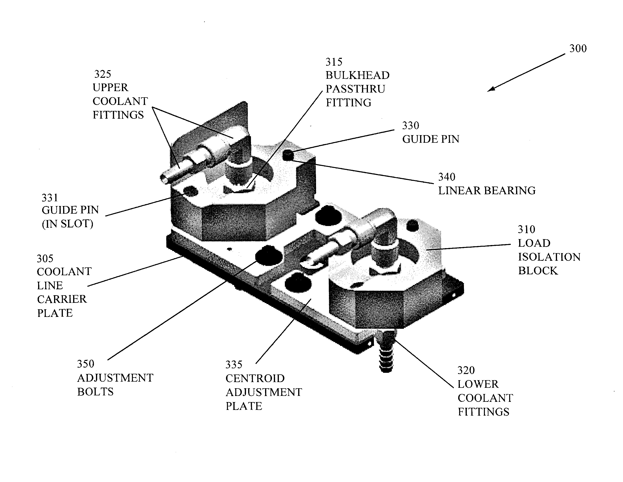
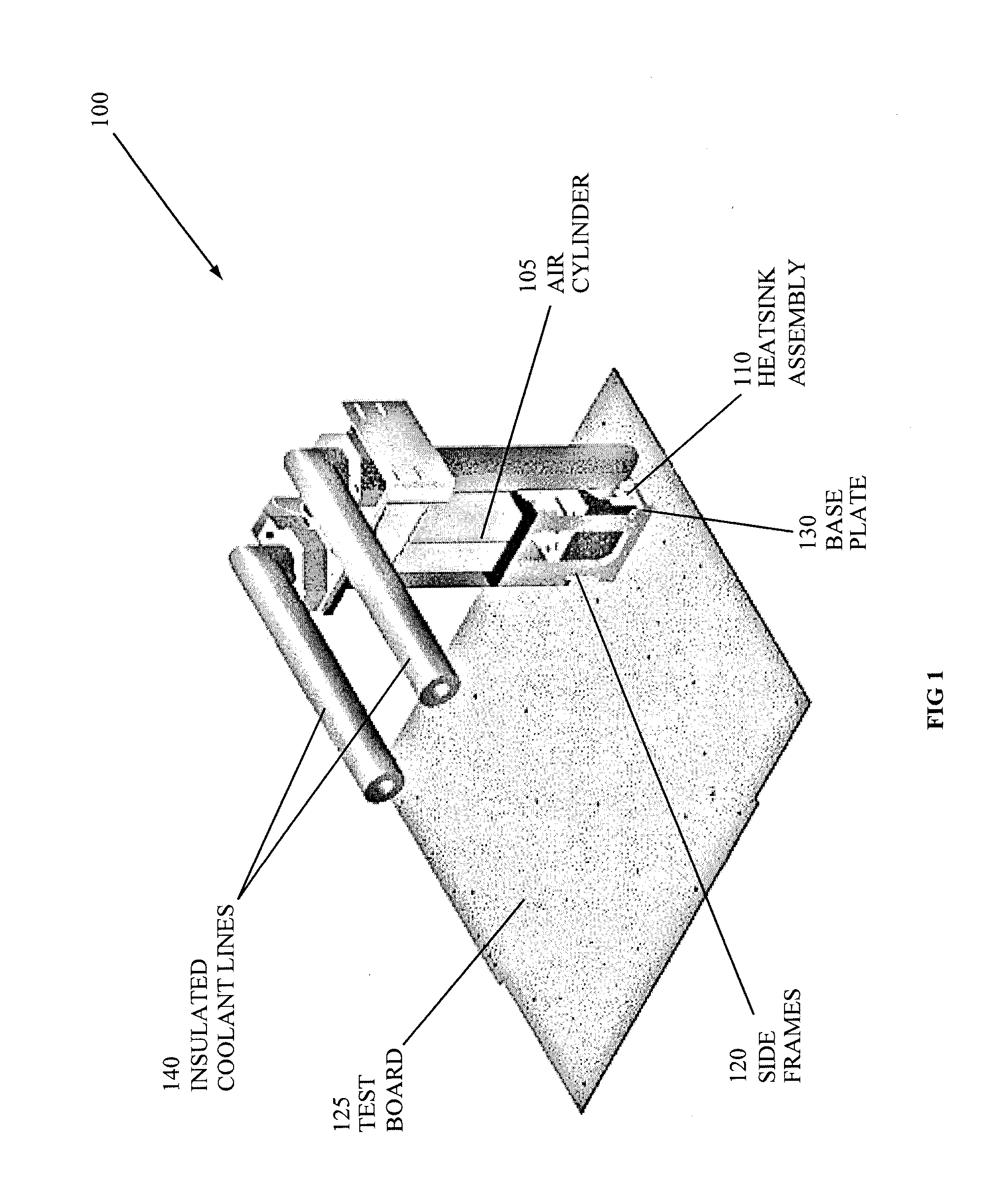
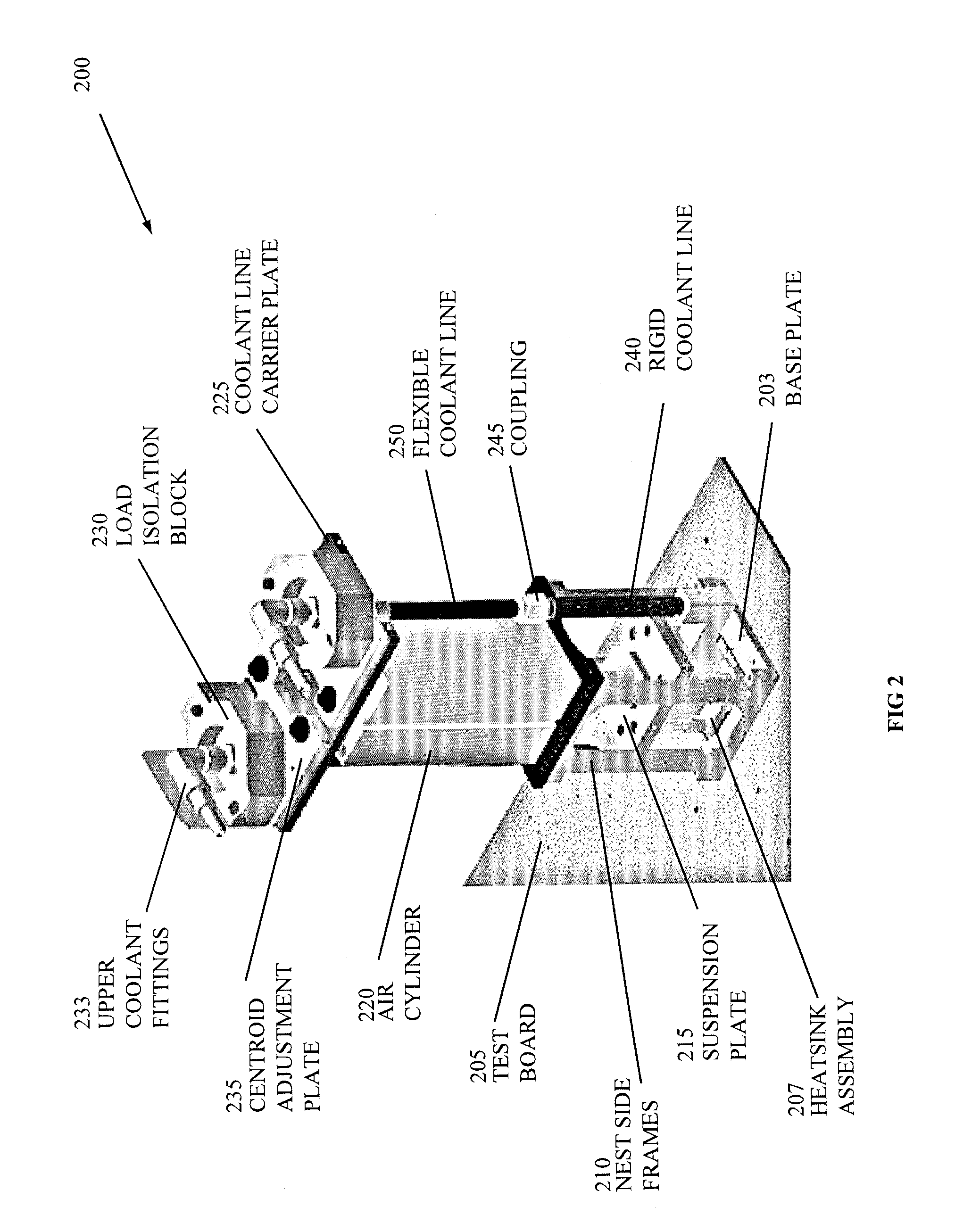
For example, nests are unnecessarily cumbersome, a problem which results in a disproportionately large nest footprint, and, thereby, seizes otherwise useable and valuable test volume; the cumbersome nest architecture also lends itself to unnecessary difficulties in installation and replacement of test sockets.
In addition, testers often have external parasitic loads and moments acting on the heatsink and chip surface without having an ability to isolate and / or adjust these loads and moments; as a result, deviations from the chip's true performance metrics, especially those related to temperature, are likely to occur for the DUT.
Another problem in the current state of the art is the effect of inattentiveness to controlling condensation on the DUT, wherein, condensation may cause damage to the tester.

Method used


Image

  • Functional and stress testing of LGA devices
  • Functional and stress testing of LGA devices
  • Functional and stress testing of LGA devices

Examples


Embodiment Construction

[0021] The following is a detailed description of example embodiments of the invention depicted with assistance and reference to the accompanying drawings. The embodiments are examples and are in such detail as to clearly communicate the invention. However, the amount of detail offered is not intended to limit the anticipated variations of embodiments; on the contrary, the intention is to cover all modifications, equivalents, and alternatives falling within the spirit and scope of the present invention as defined by the appended claims. The detailed descriptions below are designed to make such embodiments obvious to a person of ordinary skill in the art.

[0022] Generally speaking, improved systems, methods, and apparatuses for testing modules, e.g., TCA, SCM, and MCM, in an LGA socket within a tester's nest section are contemplated. As a preliminary matter, although this disclosure discusses exposed chip LGA devices, it is understood that this disclosure equally applies, extends, an...


PUM


Abstract

Improved methods, systems, and apparatuses are disclosed for testing LGA devices. One example embodiment include vertical routing of test nest assembly cooling lines in order to minimize the test nest footprint and increase available test sites on a single test card. Another example embodiment includes isolating and adjusting external loads and moments into the heatsink / cold plate, wherein these loads and moments involve controlling the centroid to restore more ideal thermal performance of the heatsink / chip interface. Still another example embodiment includes a nest architecture facilitating easy and low-cost replacement of LGA sockets. Finally, another example embodiment includes efficient condensation control of test nest assembly parts by using dry-air exhaust.

Description

CROSS REFERENCE [0001] This application is a divisional application of U.S. patent application Ser. No. 11 / 033,935 entitled IMPROVED FUNCTIONAL AND STRESS TESTING OF LGA DEVICES, attorney docket number AUS920041055US1 (4095), filed Jan. 12, 2005, the disclosure of which is incorporated herein in its entirety for all purposes.FIELD OF INVENTION [0002] The invention generally relates to functional and stress testing of land grid array (LGA) devices, and, in particular, to improved apparatuses, methods and systems therefor in relation to a module, which is the device under test, i.e., DUT. BACKGROUND [0003] Prior to installation in machines, manufacturers and assemblers, for instance, often test processor chips (“chips”) to determine their performance metrics. These metrics involve investigating chip performance using functional and non-functional test sequences throughout predetermined windows, e.g., operational, for several variables, including chip voltage, clock speed, power and te...

Claims


Application Information

Patent Timeline
Patent Type & Authority Applications(United States)
IPC IPC(8): G01R31/28
CPCG01R31/2891
Inventor CORBIN, JOHN SAUNDERS JR.GARZA, JOSE ARTUROKENT, DALES MORRISONLARSEN, KENNETH CARLMAHANEY, HOWARD VICTOR JR.PHAN, HOA THANHSALAZAR, JOHN JOSEPH
Owner IBM CORP
Learn More