
Semiconductor memory device including memory cell without capacitor

a memory cell and capacitor technology, applied in the field of semiconductor memory devices, can solve the problems that the memory cell using a capacitor becomes an obstacle in the reduction of the layout of the semiconductor memory devices, and achieve the effect of reducing the layout of the memory devi

Inactive Publication Date: 2007-08-23
SAMSUNG ELECTRONICS CO LTD
View PDF6 Cites 18 Cited by
  • Summary
  • Abstract
  • Description
  • Claims
  • Application Information

AI Technical Summary

Benefits of technology

[0047]The controller can comprise: a row decoder configured to decode a first row address of the externally applied addresses during the read operation to enable one word line of the first and second word lines and one reference word line of the first and second reference word lines corresponding to the one word line; a bit line selection signal generator configured to receive a second row address of the externally applied addresses during the read operation to output the bit line selection signal configured to select the first, second, th

Problems solved by technology

However, as the integration density of semiconductor memory devices increases, a memory cell using a capacitor becomes an obstacle in decreasing the layout of the semiconductor memory devices.
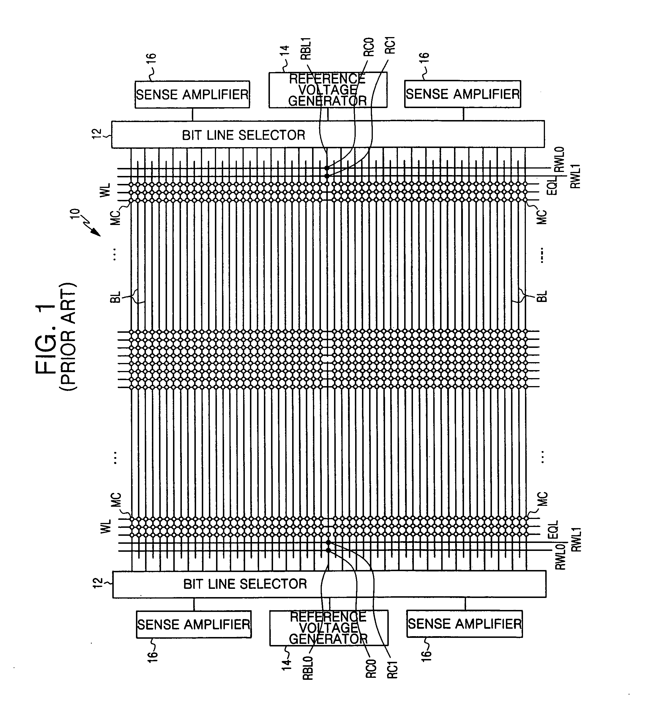
In addition, currents corresponding to data of the reference memory cells RC0 and RC1 and the memory cell MC may vary with a change in fabrication process, voltage, or operating temperature, so that an error in data sensed by the sense amplifier 16 may result.

Method used


Image

  • Semiconductor memory device including memory cell without capacitor
  • Semiconductor memory device including memory cell without capacitor
  • Semiconductor memory device including memory cell without capacitor

Examples


Embodiment Construction

[0059]It will be understood that, although the terms first, second, etc. may be used herein to describe various elements, these elements should not be limited by these terms. These terms are used to distinguish one element from another, but not to imply a required sequence of elements. For example, a first element can be termed a second element, and, similarly, a second element can be termed a first element, without departing from the scope of the present invention. As used herein, the term “and / or” includes any and all combinations of one or more of the associated listed items.

[0060]It will be understood that when an element is referred to as being “connected” or “coupled” to another element, it can be directly connected or coupled to the other element or intervening elements may be present. In contrast, when an element is referred to as being “directly connected” or “directly coupled” to another element, there are no intervening elements present. Other words used to describe the r...


PUM


Abstract

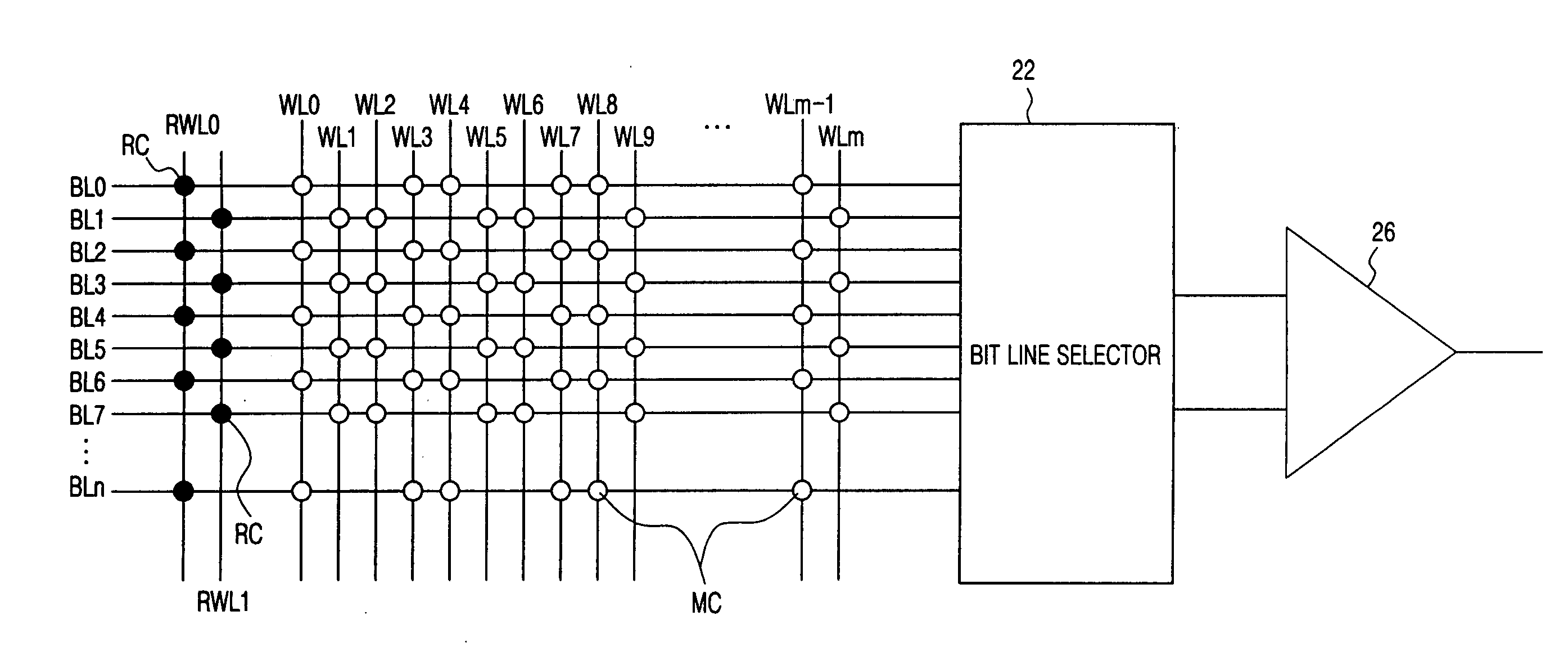
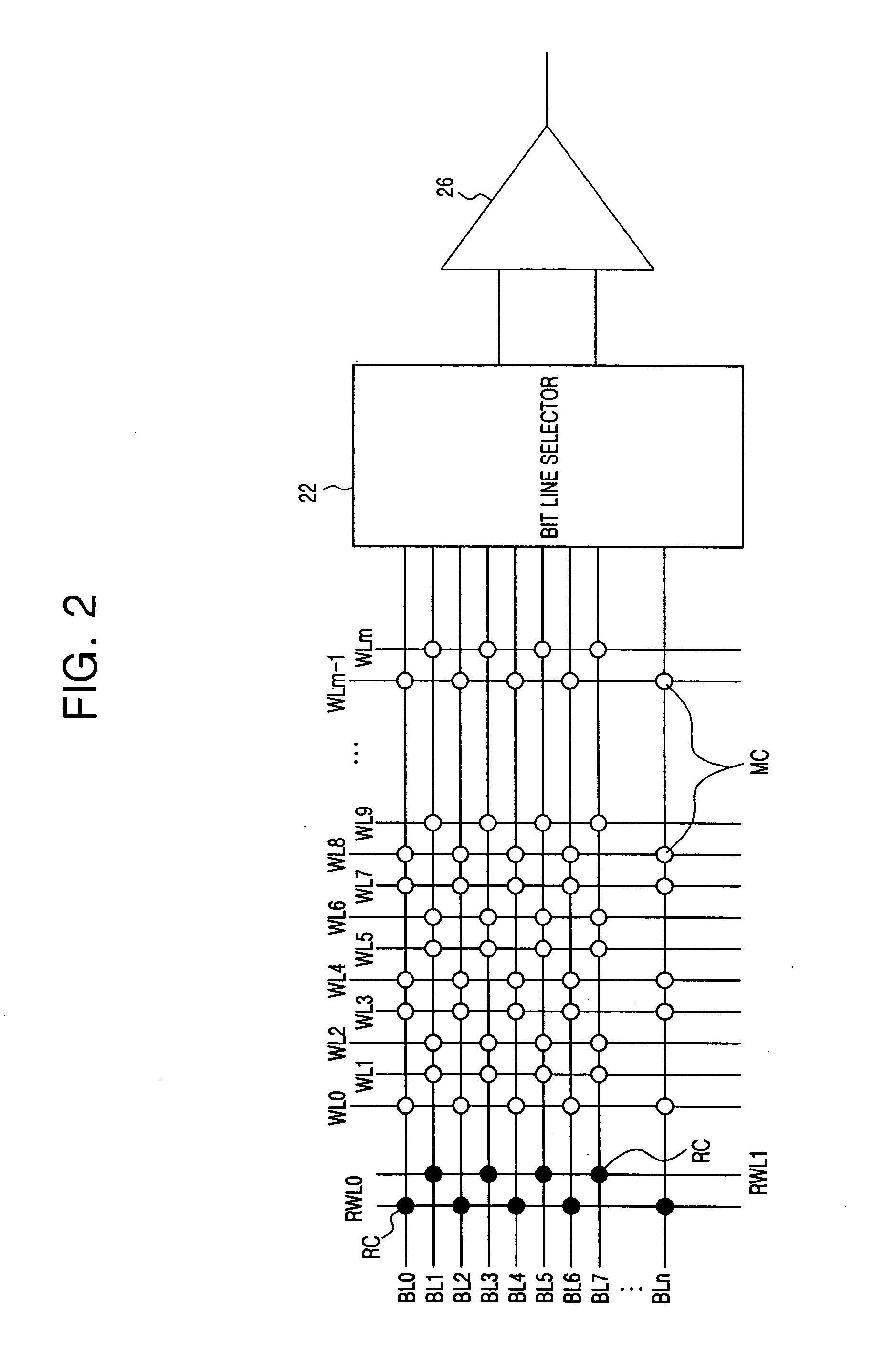
A semiconductor memory device including a memory cell without a capacitor includes: a memory cell array block including first memory cells connected between a first bit line and first word lines and second memory cells connected between a second bit line and second word lines; and a reference memory cell array block including first reference memory cells connected between a first reference bit line connected to the first bit line and a first reference word line and second reference memory cells connected between a second reference bit line connected to the second bit line and a second reference word line. When the first word lines are selected, the second reference memory cells are selected, and when the second word lines are selected, the first reference memory cells are selected. Thus, each bit line includes a reference memory cell and outputs reference signal from the reference memory cell so that data can be precisely sensed during a read operation.

Description

[0001]This application claims priority to Korean Patent Application No. 10-2006-0016936, filed Feb. 21, 2006, the contents of which are hereby incorporated herein by reference in their entirety.BACKGROUND OF THE INVENTION[0002]1. Field of the Invention[0003]The present invention relates to a semiconductor memory device and, more particularly, to a semiconductor memory device including a memory cell without a capacitor in which a dynamic memory cell includes a single transistor with a floating body.[0004]2. Description of Related Art[0005]In general, a dynamic random access memory (DRAM) device, which is one type of semiconductor memory device, includes a memory cell that is comprised of a transistor and a capacitor, so that data “0” or “1” is determined depending on whether or not the capacitor is electrically charged. That is, a conventional DRAM device needs a capacitor to store data. However, as the integration density of semiconductor memory devices increases, a memory cell usin...

Claims


Application Information

Patent Timeline
IPC IPC(8): G11C7/02
CPCG11C7/14G11C7/18G11C2211/4016G11C11/4097G11C11/4099G11C11/404G11C7/06G11C11/4091
Inventor KIM, JIN-YOUNGLEE, YEONG-TAEK
Owner SAMSUNG ELECTRONICS CO LTD
Learn More