System and method for determining probing locations on IC

a technology of probing location and system, applied in the direction of testing circuits, semiconductor/solid-state device testing/measurement, instruments, etc., can solve the problems of difficult to determine the corresponding circuit element that is probed, difficult to determine the corresponding circuit element that emits light, and inconvenient to determine the corresponding circuit elemen

Inactive Publication Date: 2007-08-02
DCG SYST
View PDF3 Cites 22 Cited by
  • Summary
  • Abstract
  • Description
  • Claims
  • Application Information

AI Technical Summary

Benefits of technology

[0018] According to still another aspect of the invention, a computerized system for determining locations on an integrated circuit microchip to be probed and controlling a stage to place a prober at the proper location is provided. The system comprising a computer having an input, an output, and a processor. The processor is pre-programmed to perform the steps: a. receive via the input a callout list of failures, the callout list including cell name and pin for each failure; b. interrogate a Def file to locate a Def entry matching the cell name and obtain from the Def entry cell type, cell location, and cell orientation data; c. interrogate a Lef file to locate a Lef entry matching the cell type and obtain from the Lef entry coordinates of the pin; d. interrogate a GDS file to locate a GDS entry matching the cell type and obtain coordinates of polygons listed in the GDS entry; and e. determine from the interrogated files the proper location on the microchip to be probed. The system then provides an output to control the motion of a stage so as to align the prober with the location on the microchip.

Problems solved by technology

As can be understood, the methods used in the prior art to arrive at probing locations are tedious and time consuming.
Conversely, in cases where a fault location is detected by the prober, it is currently difficult to determine the corresponding circuit element that is probed.
However, the prober provides no information with respect to layout or circuit design of the DUT, so that the circuit element that emits the light is not readily identifiable. FIG. 1B depicts a general process of the prior art for determining the circuit element that may be responsible for the emission spot.

Method used


Image

  • System and method for determining probing locations on IC
  • System and method for determining probing locations on IC
  • System and method for determining probing locations on IC

Examples


Embodiment Construction

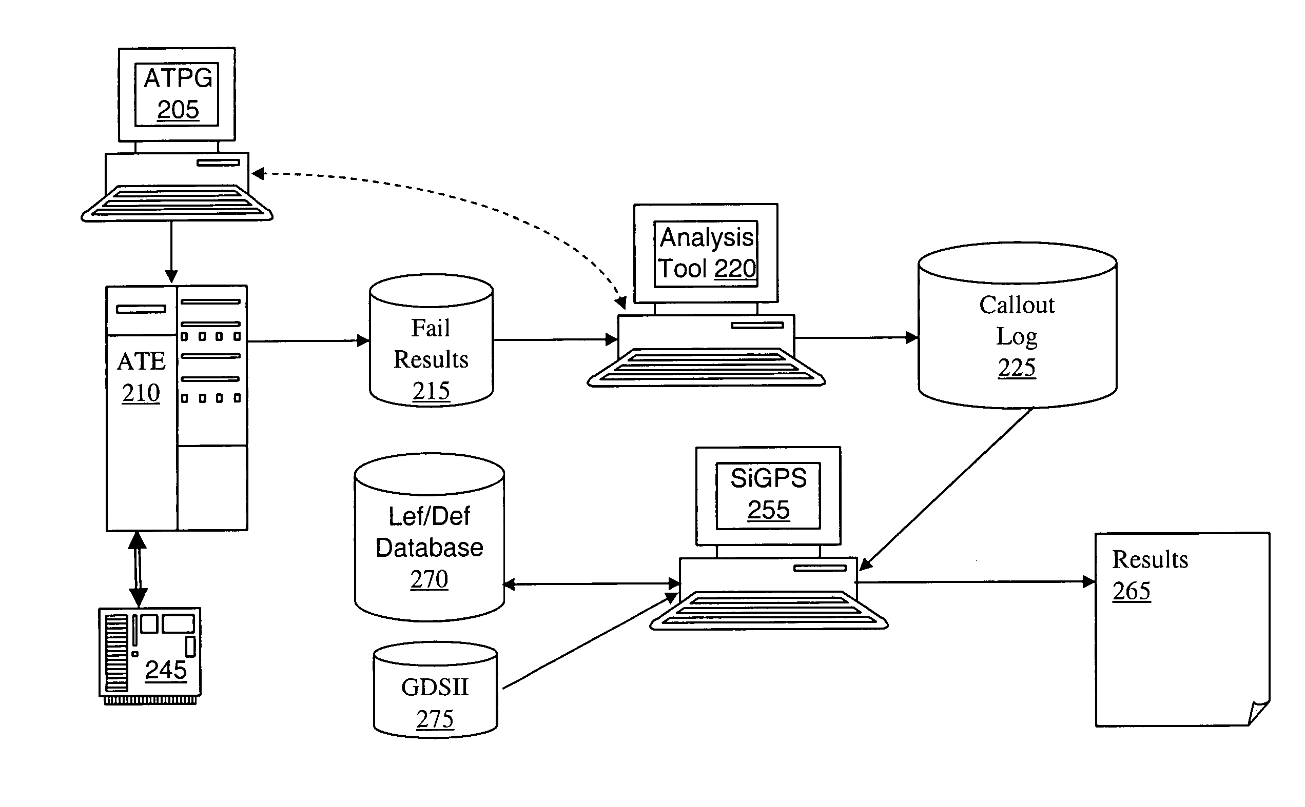
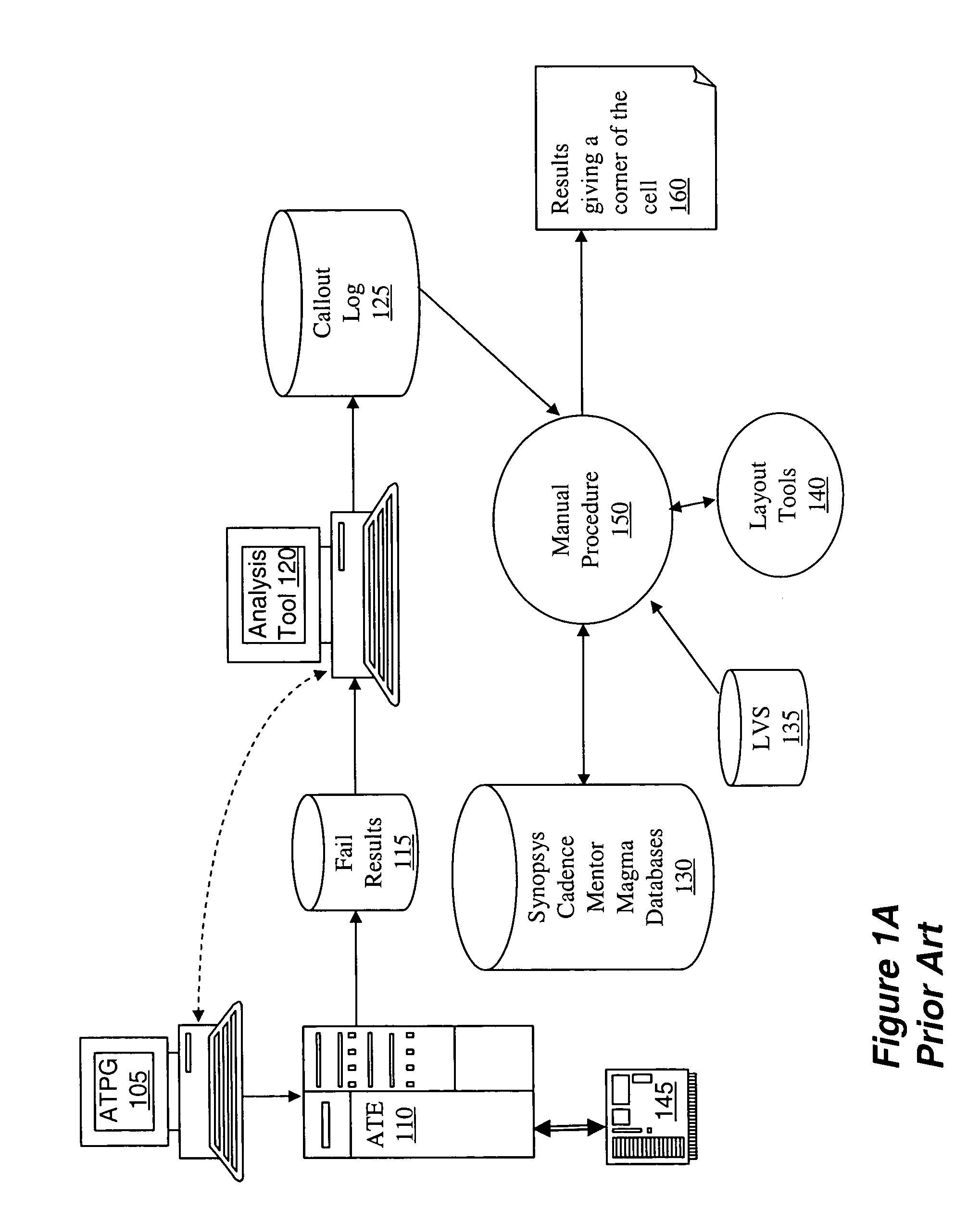
[0045]FIG. 2 depicts an embodiment of the present invention. In this embodiment, all of the equipment and processes leading to the generation of the callout log 225 are the same as in the prior art. However, according to this embodiment, The Def / Lef and GDSII files are interrogated to produce the results of locations for probing, providing the bounding box of the cell, the pins, and the locations within the cell where TRE probing may be performed. This process is referred to herein as SiGPS and may be done automatically using a specifically programmed computer, such as a PC.

[0046] The terms Lef, Def, and GDS are commonly used in the art. Due to increasing size and complexity of the designs, engineers use automated tools to do the floor planning followed by place and route (P&R). During the P&R stage, the design tools have the ability to generate LEF / DEF files. These files are in ASCII format and contain the place and route data. The term Lef is an acronym for Library Exchange Forma...


PUM


Abstract

An apparatus and method for tracing back a probing location to identify the circuit element being probed on a device under test (DUT). The coordinates of the irregularity on the DUT are used to trace back to the logic cone to decipher the root-cause of the irregularity. The Def and Lef files are interrogated using the coordinates to obtain the cell and net data to enable the investigation. Additionally, a schematic viewer is used to investigate the logic cone to potential root-causes for the irregularities.

Description

CROSS-REFERENCE TO RELATED APPLICATIONS [0001] This application claims priority from, and is a continuation in part of U.S. application Ser. No. 11 / 345,004, filed Jan. 31, 2006 and commonly assigned to the current assignee, and which is incorporated herein by reference in its entirety. This case also claims priority from U.S. application Ser. No. 60 / 774,991, filed Feb. 17, 2006, which is incorporated herein by reference in its entirety.BACKGROUND [0002] 1. Field of the Invention [0003] The present invention relates to an apparatus and method for finding exact locations for probing integrated circuits, and conversely tracing the circuit element and location of a suspected spot on a DUT (device under test) probed by a probing tool. [0004] 2. Description of the Related Art [0005] Probing systems have been used in the art for testing and debugging integrated circuit (IC) designs and layouts. Various laser-based systems for probing IC's are known in the prior art. In these prior art syst...

Claims


Application Information

Patent Timeline
Patent Type & Authority Applications(United States)
IPC IPC(8): G01R27/28G01R31/00
CPCG01R31/31704G01R31/311
Inventor SURI, HITESHKARDACH, CATHY
Owner DCG SYST
Why Eureka
Try Eureka