
Double encapsulated semiconductor package and manufacturing method thereof

a semiconductor and packaging technology, applied in the field of semiconductor packaging, can solve the problem of additional costs in manufacturing a mold di

Inactive Publication Date: 2007-07-19
SAMSUNG ELECTRONICS CO LTD
View PDF2 Cites 25 Cited by
  • Summary
  • Abstract
  • Description
  • Claims
  • Application Information

AI Technical Summary

Benefits of technology

The present invention provides a way to make a double encapsulated semiconductor package without needing to create a new mold die. This is achieved by attaching a complex chip with normal and random pads to a wiring substrate with windows for the pads to be exposed. The pads are then connected to the substrate using bonding wires. The chip and substrate are covered with separate resin encapsulation portions, with the first one being formed by a molding method and covering the chip and windows on the substrate, and the second one being formed by a potting method and covering the windows on the substrate. This method allows for efficient and cost-effective production of semiconductor packages.

Problems solved by technology

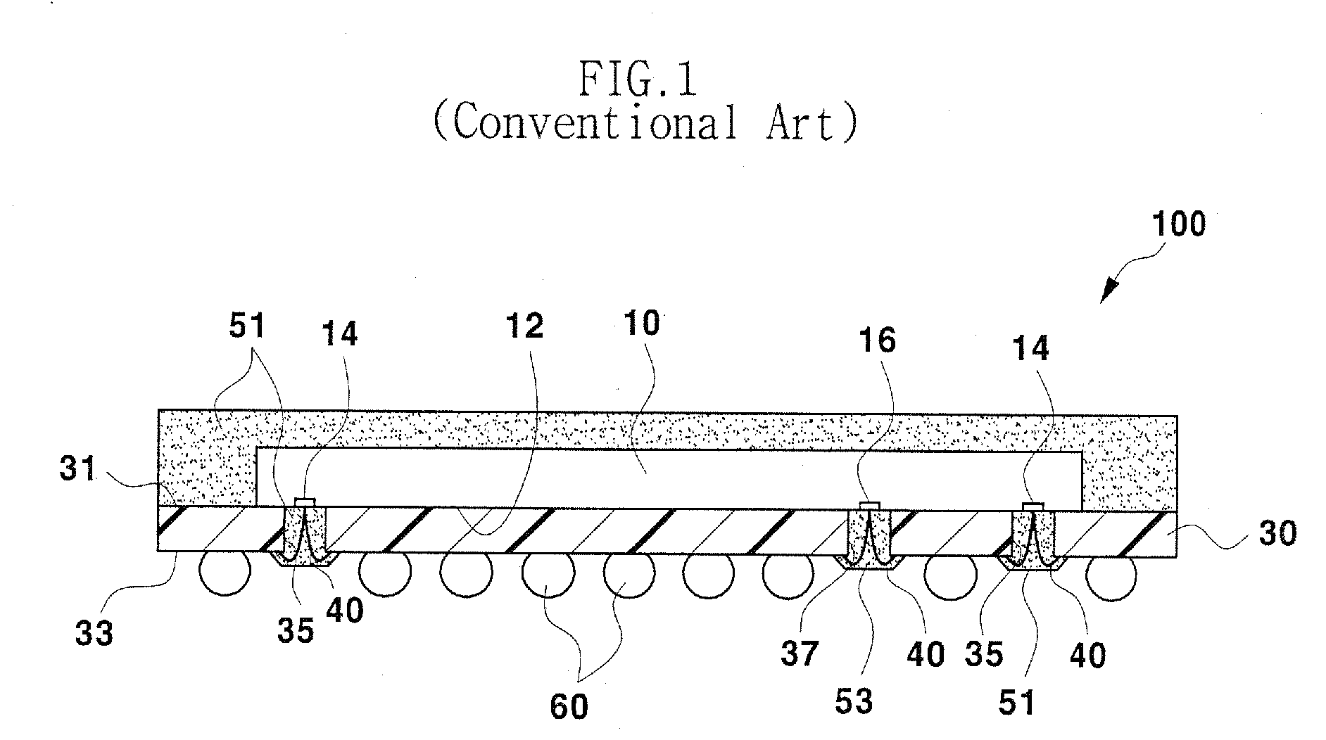
Therefore additional costs may arise in manufacturing a mold die having a runner corresponding to the locations of the second windows 37.

Method used


Image

  • Double encapsulated semiconductor package and manufacturing method thereof
  • Double encapsulated semiconductor package and manufacturing method thereof
  • Double encapsulated semiconductor package and manufacturing method thereof

Examples


example 1

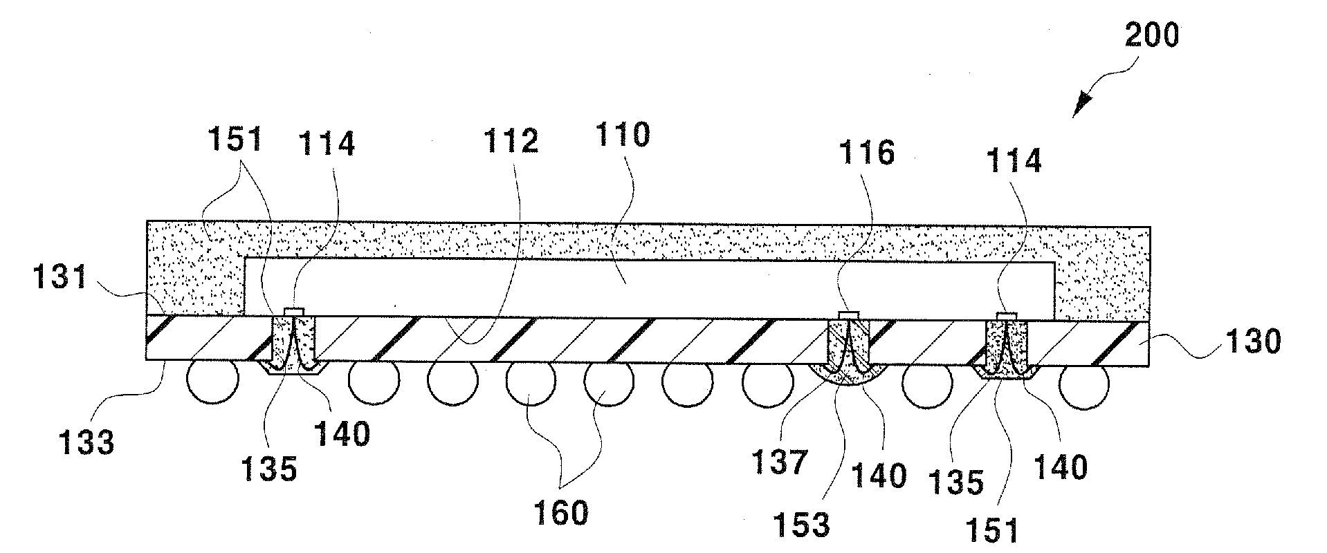
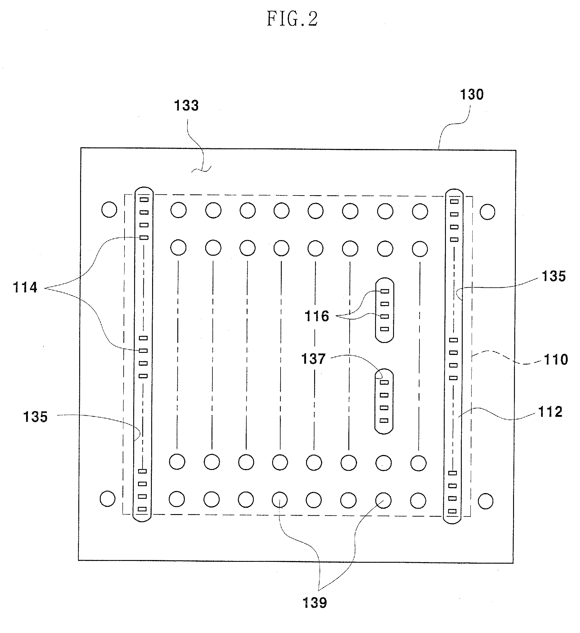
[0022]FIG. 2 is a plan view showing a wiring substrate 130 of a double encapsulated semiconductor chip according to a first example embodiment of the present invention. FIG. 3 is a plan view showing the double encapsulated semiconductor package 200 according to the first example embodiment of the present invention. FIG. 4 is a sectional view taken along the line IV-IV of FIG. 3.

[0023]Referring to FIGS. 2 to 4, the semiconductor package 200 according to the first example embodiment of the present invention is a BOC package in which a complex chip 110 is attached to the wiring substrate 130 in a face-down form.

[0024]The complex chip 110 includes normal pads 114 that may be formed at both sides of an active surface 112 and random pads 116 that may be formed at an inner area of the active surface 112. The normal pads 114 may be formed at both sides parallel to each other and the random pads 116 may be formed in two groups that maintain a predetermined distance between each other.

[0025]T...

example 2

[0045]Although, in the first example embodiment of the present invention, an example where normal pads of a complex chip are formed in an edge pad type is illustrated, the normal pads may also be formed in a center pad type as shown in FIG. 8. A semiconductor package 300 according to a second example embodiment of the present invention has the same structure as that of the first example embodiment from the viewpoint that a complex chip 210 is attached to a first surface 231 of a wiring substrate 230 in a face-down manner.

[0046]Normal pads 214 of the complex chip 210 are formed at a center area of an active surface 212, and random pads 216 of the complex chip 210 are formed outside the center area of the active surface 212. First windows 235 and second windows 237 are formed such that the first windows 235 and second windows 237 correspond to the normal pads 214 and the random pads 216 of the complex chip 210, respectively, in the wiring substrate 230. Additionally, a first resin enc...

example 3

[0048]Although, in the first and second example embodiments of the present invention, examples of semiconductor package installed with a single complex chip have been illustrated, a semiconductor package 400 installed with normal chips 321 and 325, and a complex chip 310 may be provided in a multi-chip form as shown in FIG. 9.

[0049]The semiconductor package 400 according to a third example embodiment of the present invention is a multi-chip package having a first normal chip 321 and a complex chip 310 installed horizontally on a first surface 331 of a wiring substrate 330, and a normal chip 325 vertically stacked on the first normal chip 321 and the complex chip 310.

[0050]The complex chip 310 and the first normal chip 321 are attached on the first surface 331 of the wiring substrate 330 maintaining a predetermined distance between each other. The first normal chip 321 mat be a semiconductor chip with an edge pad type formed with normal pads 323 at both sides of an active surface 322...


PUM


Abstract

A double encapsulated semiconductor package and manufacturing methods of forming the same are provided. Embodiments of the semiconductor package include a complex chip having normal and random pads formed on its active surface, the complex chip being attached to a first surface of a wiring substrate. First and second windows are formed in the wiring substrate to respectively expose the normal and random pads, and to allow bonding wires to be connected to the normal and random pads with the wiring substrate. A first resin encapsulation portion is formed by a molding method in the first window and a second resin encapsulation portion is formed by a potting method in the second window.

Description

PRIORITY STATEMENT[0001]This U.S. non-provisional application claims benefit of priority under 35 U.S.C. §119 from Korean Patent Application No. 2006-4298, filed on Jan. 16, 2006, the entire contents of which are incorporated by reference.BACKGROUND[0002]1. Field of the Invention[0003]The present invention relates to a semiconductor package, and more particularly, to a semiconductor package and a manufacturing method thereof having resin encapsulation portions formed at both sides of a wiring substrate.[0004]2. Description of the Prior Art[0005]In the current market of electronic products demand for mobile electronic products is rapidly increasing, and miniaturization of parts used in the electronic products is essential for satisfying this demand. A technology for reducing the size of an individual semiconductor package installed as a part, a system on chip (SOC) technology making a plurality of semiconductor chips into one chip, or a system in package (SIP) technology integrating ...

Claims


Application Information

Patent Timeline
Patent Type & Authority Applications(United States)
IPC IPC(8): H01L23/495
CPCH01L23/3128H01L2224/32145H01L25/0652H01L25/0657H01L2224/48091H01L2224/4824H01L2224/49109H01L2225/0651H01L2924/01005H01L2924/01014H01L2924/01015H01L2924/01028H01L2924/01033H01L2924/01079H01L2924/01082H01L2924/15311H01L24/49H01L2224/06136H01L2224/06135H01L2924/014H01L2924/01006H01L24/48H01L2924/00014H01L2924/00H01L2924/181H01L2924/15151H01L2224/45099H01L2224/05599H01L2924/00012H01L23/28
Inventor JUN, BYUNG-SEOKKIM, GIL-BEAGLEE, YONG-JIN
Owner SAMSUNG ELECTRONICS CO LTD
Learn More