Circuit and method for amplification of an electrical input signal

a technology of circuit arrangement and circuit arrangement, applied in the direction of amplifier combinations, gain control, instruments, etc., can solve the problems of increasing power loss in the circuit arrangement, and amplification stages that require different currents. achieve the effect of simple and cost-effectiv

Inactive Publication Date: 2007-07-12
SIEMENS HEATHCARE GMBH
View PDF3 Cites 6 Cited by
  • Summary
  • Abstract
  • Description
  • Claims
  • Application Information

AI Technical Summary

Benefits of technology

[0009] An object of the present invention is to provide a circuit arrangement and a method of the aforementioned type in which the problems described above are avoided or at least reduced in a simple and cost-effective manner.
[0013] The inventive controller has the advantage that if the current requirement of the first amplification stage is greater than the current requirement of the second amplification stage, the amplification of the first partial signal is reduced because the amplification of the first amplifier is dependent on the difference between the two currents. A lower amplification accompanies a lower output power and a lower current requirement. Since in reverse the amplification of the second amplification stage is a function of the negative current difference, i.e. of the first supply current minus the second supply current, the amplification of the second partial signal is increased. The second amplification stage thus generates a higher output power and requires a higher supply current.
[0015] In the equilibrium state, since they require the same currents both amplification stages have the same junction temperature and thus also the same difference from the maximum allowable junction temperature. This allows each amplification stage to operate with the highest possible operating current and consequently with the maximum possible (and nevertheless safer) junction temperature. In spite of maximum output power, the risk is thereby reduced (or even entirely avoided) of a too-early monitoring alarm activation or even an automatic deactivation of an amplification stage occurring due to overheating of one of the amplification. stages. Expensive additional cooling thus is not required. As a secondary effect, power losses in the recombination of the signals are reduced or minimized because the output powers of both amplification stages in the circuit arrangement are kept equal.
[0016] In an embodiment of the invention, the signal splitter effects a phase shift of the partial signals relative to one another. In this embodiment of the invention, the signal combination element resets the phase shift with the same amplitude. This means that, if the signal splitter implements a phase shift of the first partial signal relative to the second partial signal (for example by 180°), the signal combination element implements a phase shift of the first partial signal relative to the second partial signal by −180° before the recombination of the partial signals. This can be achieved by suitable delay elements at the output of the signal splitter and at the input of the signal combination element. By means of such a phase shift, a better decoupling of both parallel amplification stages from one another is achieved.
[0017] In a particularly advantageous embodiment, the relative phase shift between the partial signals amounts to 90°. Crosstalk or over-coupling of the one partial signal with the other partial signal upon the recombination is avoided as far as it is possible and the two amplification stages are insensitive relative to load changes at the output, which could be caused by reflections from the signal combination element.
[0026] Such a cascade-like design can be executed in two stages (but also in multiple stages) by the amplification stages within the subordinate circuit arrangement themselves being designed as inventive circuit arrangements. This means that it is possible in the inventive manner to use not only two but also four, eight, sixteen, thirty-two or more individual semiconductor amplification stages within the entire circuit arrangement. Nearly arbitrarily high output powers can thereby be achieved.

Problems solved by technology

One problem is that such amplification stages should not be operated above a maximum barrier layer temperature (junction temperature) of the transistors since this can lead to a premature failure of the amplification stage.
Due to tolerances in the transistors, it disadvantageously occurs that the amplification stages require different currents.
This mechanism leads on the one hand to a situation that the power loss in the circuit arrangement increases and its efficiency consequently decreases.
It can additionally lead to an asymmetrical output power of the individual amplification stages, which leads to additional power losses.
Both methods significantly increase the energy expenditure and the costs for the amplification.

Method used


Image

  • Circuit and method for amplification of an electrical input signal
  • Circuit and method for amplification of an electrical input signal
  • Circuit and method for amplification of an electrical input signal

Examples


Embodiment Construction

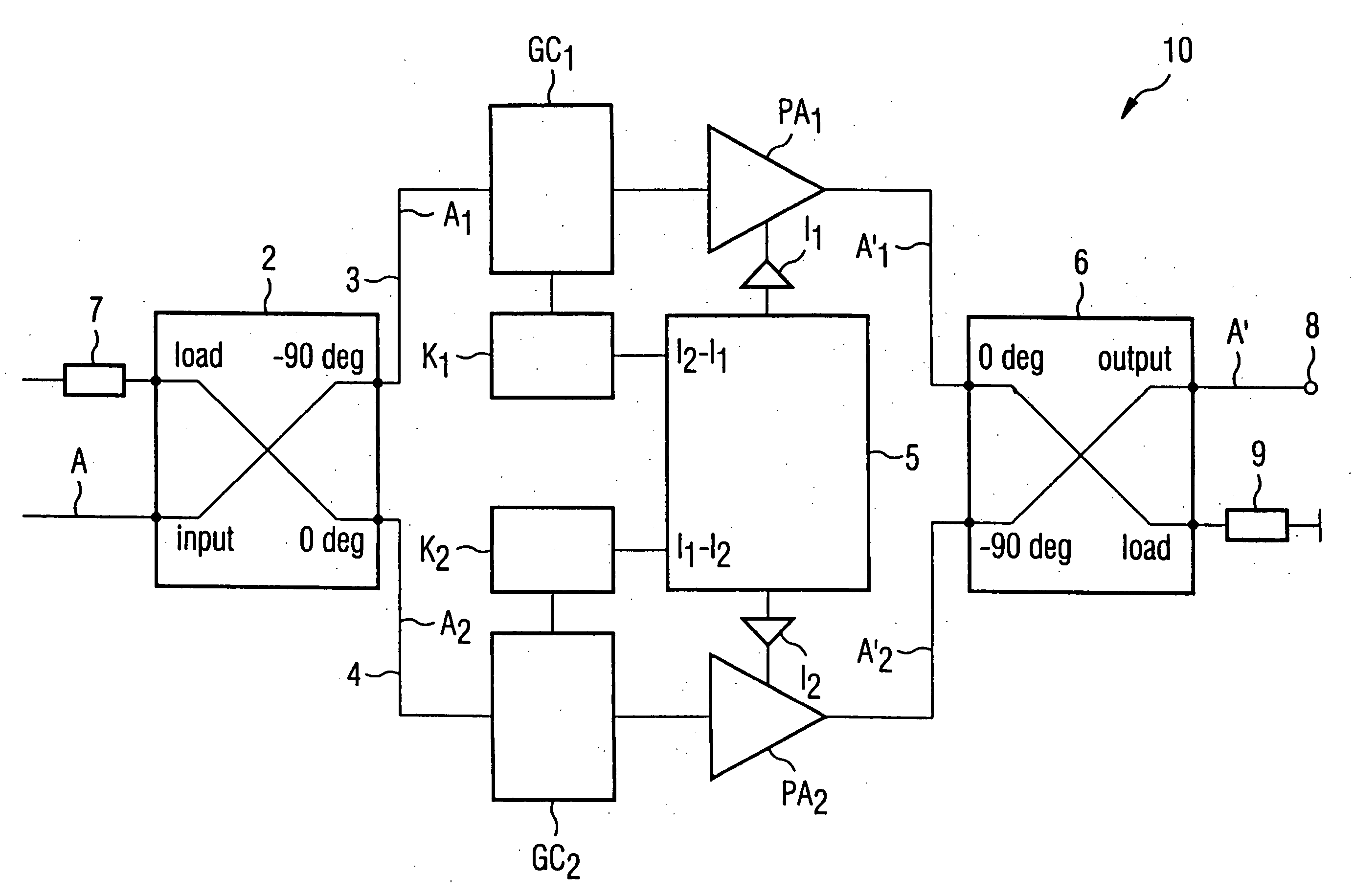
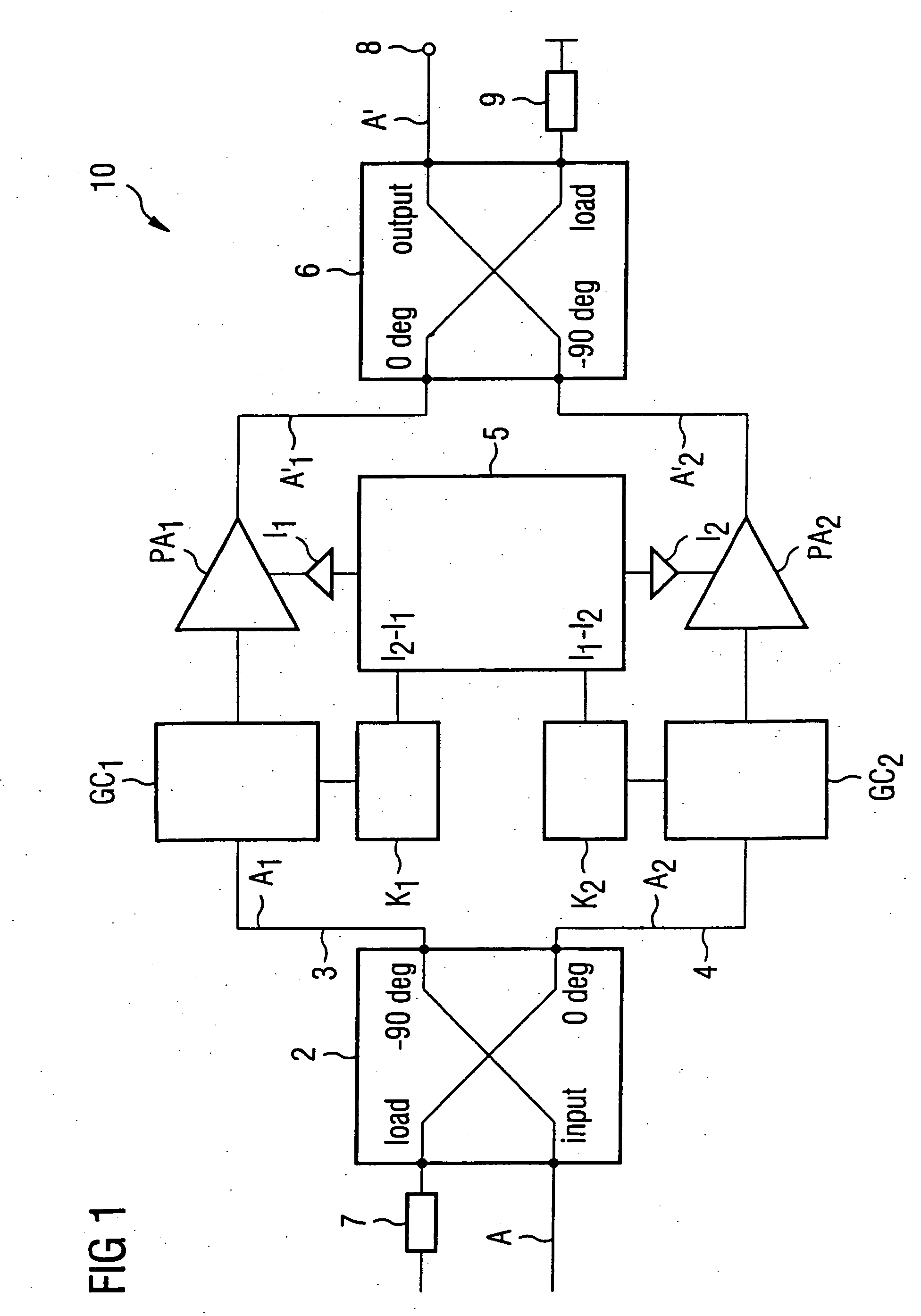
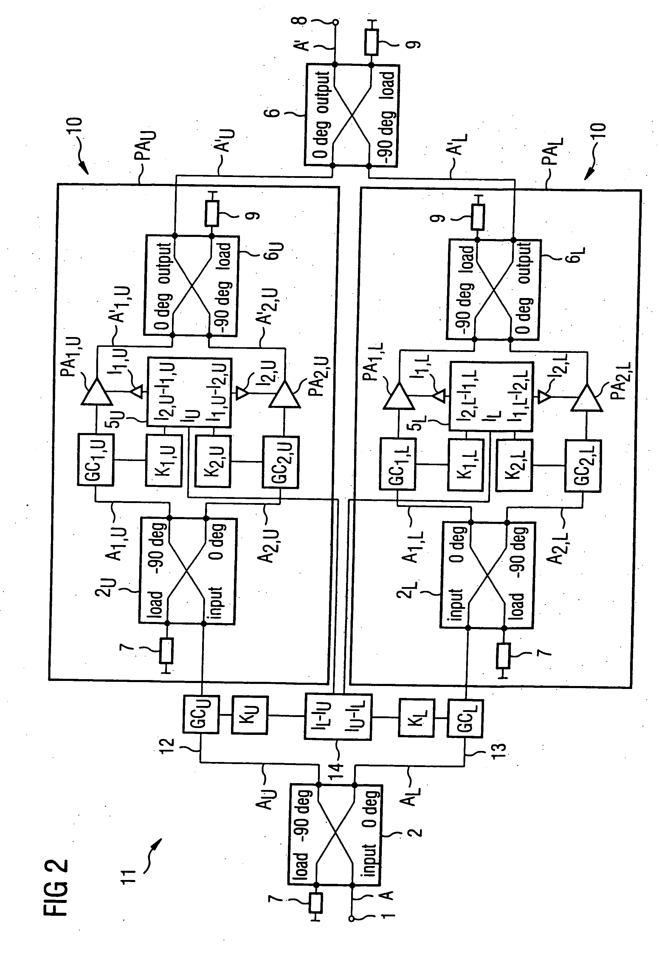
[0030] In the relatively simple exemplary embodiment shown in FIG. 1, the circuit arrangement 10 has only two connected amplification stages PA1, PA2 that are arranged in parallel to one another. These two amplification stages PA1, PA2 are formed from semiconductor power transistors. The circuit arrangement 10 is particularly suitable for amplification of radio-frequency pulses in magnetic resonance systems, which radio-frequency pulses generally being in a frequency range from 10 to 150 MHz.

[0031] On the input side, a signal splitter 2, which divides an input signal A into a first partial signal A1 and a second partial signal A2, is provided in the circuit arrangement 10, with each of the two partial signals A1, A2 exhibits half of the power of the input signal A. For this purpose, the signal splitter 2 has a signal input 1 at which the input signal A is present, a load input which is terminated by a termination resistance of, for example, 50 Ohm, and two signal outputs for the pa...


PUM


Abstract

In a circuit and a method for amplification of an electrical input signal, a signal splitter divides the input signal into a first partial signal in a first signal path and a second partial signal in a second signal path. The first signal path has a first amplification stage for amplification of the first partial signal and the second signal path has a second amplification stage for amplification of the second partial signal. Each of the two amplification stages is supplied with current by a current supply device. Both amplified partial signals are recombined into an output signal by a signal combination element downstream from the amplification stages. The first amplification stage and the second amplification stage are coupled with a regulation device that regulates the amplification of the first partial signal dependent on a current difference between a supply current requirement of the second amplification stage and a supply current requirement of the first amplification stage and which regulates the amplification of the second partial signal dependent on a current difference between the supply current requirement of the first amplification stage and the supply current requirement of the second amplification stage.

Description

BACKGROUND OF THE INVENTION [0001] 1. Field of the Invention [0002] The present invention concerns a circuit arrangement and method for amplification of an electrical input signal and a magnetic resonance system with such a circuit arrangement. [0003] 2. Description of the Prior Art [0004] Amplification circuits are known that have a signal splitter that splits the input signal into a first partial signal and a second partial signal. A first signal path has a first amplification stage for amplification of the first partial signal and a second signal path has a second amplification stage for amplification of the second signal. Each of the two amplification stages is supplied with current from a power supply device. A signal combination element downstream from the amplification stages recombines the two partial signals into one output signal. The invention furthermore concerns a corresponding method for amplification of an electrical input signal. [0005] Such circuit arrangements are ...

Claims


Application Information

Patent Timeline
IPC IPC(8): H03F3/68
CPCG01R33/3621H03F1/0211H03F3/211H03F2200/447H03G3/3042H03F2203/21142H03F2203/21181H03F2203/21184H03F2203/21187H03F2203/21106
Inventor ALBRECHT, ADAM
Owner SIEMENS HEATHCARE GMBH
Why Eureka
Try Eureka