
Semiconductor device and method of manufacturing the same

a technology of semiconductor devices and semiconductors, applied in semiconductor devices, electrical devices, transistors, etc., can solve the problems of difficult to obtain a desired hfe value, difficult to obtain hfe value immediately after, complicated manufacturing steps, etc., to achieve the effect of reducing the contact resistance of the emitter electrode, reducing the size of the device, and reducing the base width

Inactive Publication Date: 2007-06-28
SANYO ELECTRIC CO LTD
View PDF6 Cites 4 Cited by
  • Summary
  • Abstract
  • Description
  • Claims
  • Application Information

AI Technical Summary

Benefits of technology

The present invention is a semiconductor device that includes a semiconductor layer with an emitter region, a base region, and a collector region. The emitter region has a wider diffused region in a deeper portion of the semiconductor layer, which prevents free carriers from recombining on the surface of an epitaxial layer. This structure allows for a smaller base width in the deep portion of the semiconductor layer, resulting in a desired hfe value. The semiconductor device also includes a concentration gradient in the emitter region, which reduces contact resistance and allows for a smaller device size. The method of manufacturing the semiconductor device includes forming a collector region, an insulating layer, and a contact hole for the emitter region using the insulating layer as a mask, with different ion implantation conditions to form the emitter region with a large diffusion width and a small base width. Overall, the present invention provides a semiconductor device with improved performance and reduced device size.

Problems solved by technology

In particular, there is a problem that it is difficult to obtain hfe value in a minute current region immediately after the lateral PNP transistor is turned on.
Thus, there is a problem that it is difficult to obtain a desired hfe value.
Specifically, there is a problem that manufacturing steps become complicated, and that manufacturing costs are also increased.
As a result, there is a problem that a width of the contact hole is increased, and that it is difficult to reduce the device size.

Method used


Image

  • Semiconductor device and method of manufacturing the same
  • Semiconductor device and method of manufacturing the same
  • Semiconductor device and method of manufacturing the same

Examples


Embodiment Construction

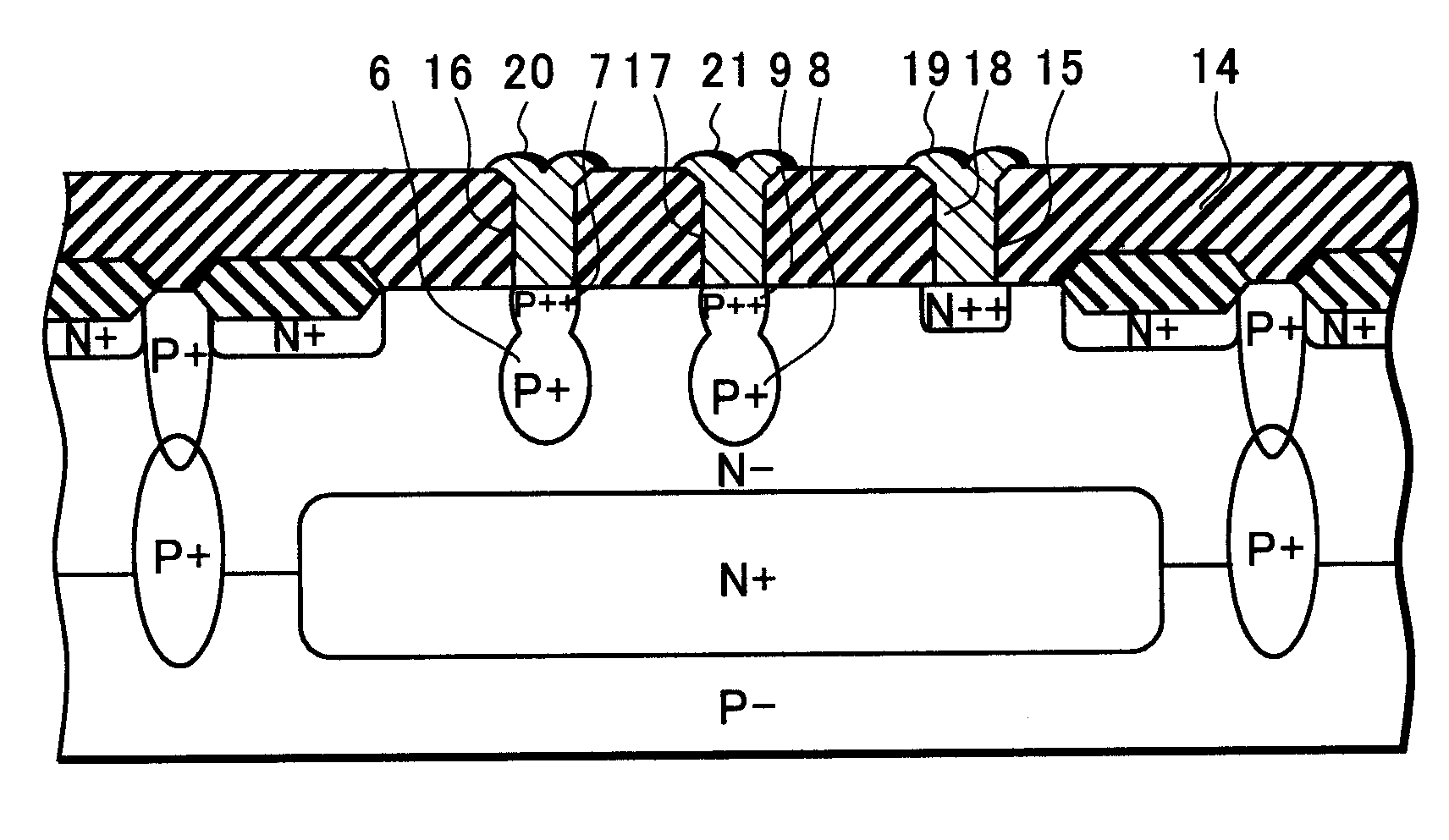
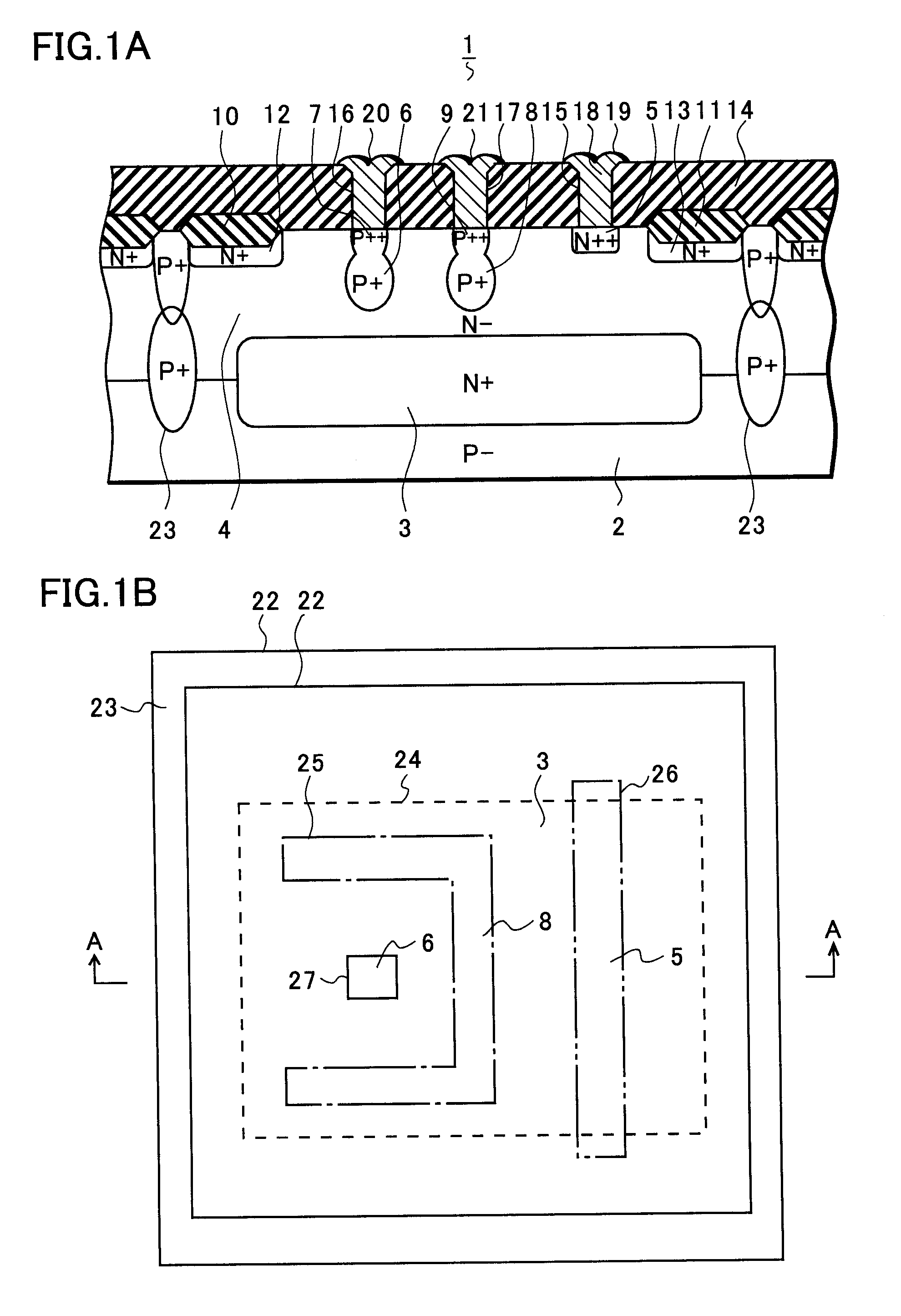
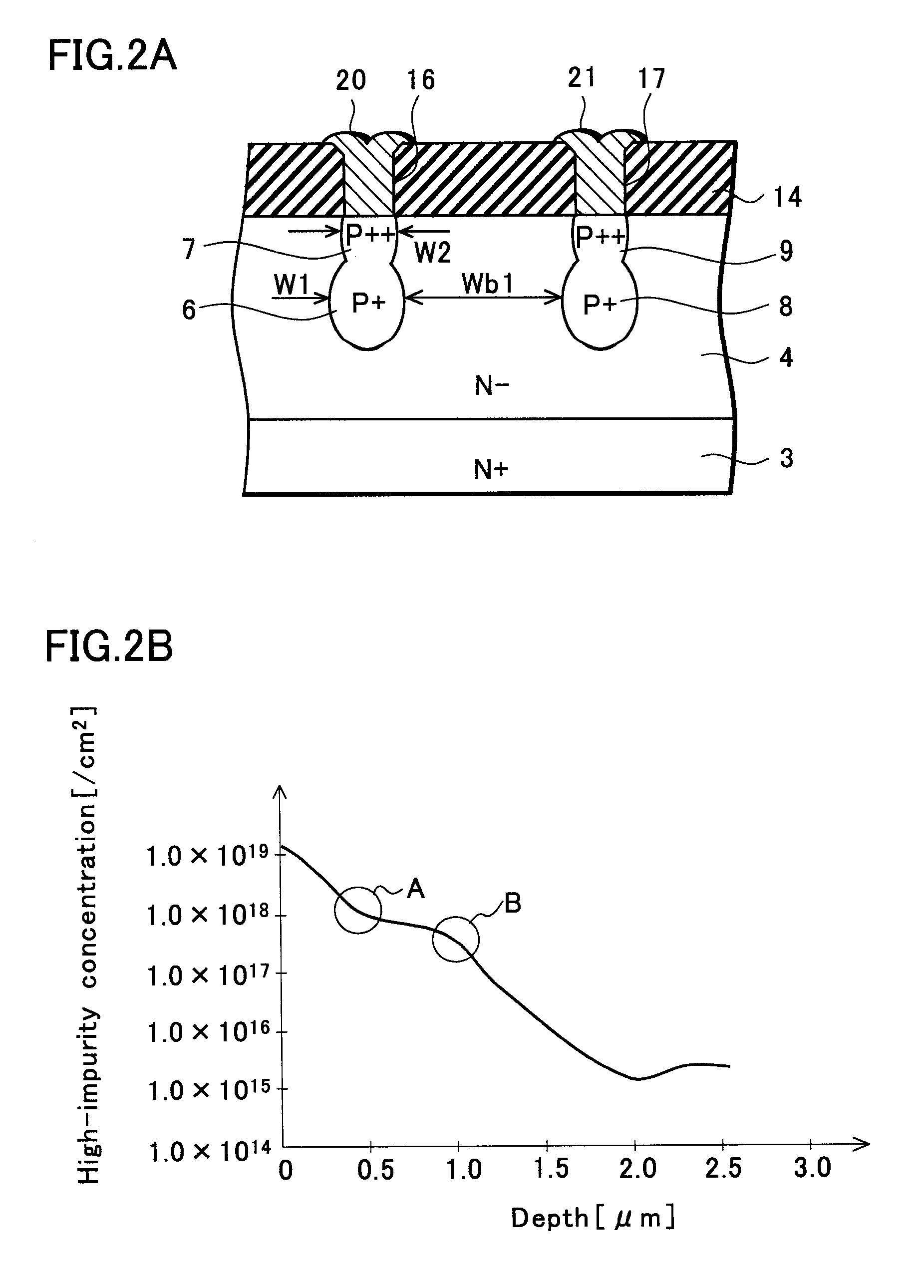
[0027] With reference to FIGS. 1 to 3, a semiconductor device according to a preferred embodiment of the present invention will be described in detail below. FIG. 1A is a cross-sectional view illustrating a semiconductor device according to the embodiment. FIG. 1B is a plan view illustrating the semiconductor device according to the embodiment. FIG. 2A is a cross-sectional view illustrating a collector region and an emitter region in the semiconductor device according to the embodiment. FIG. 2B is a graph illustrating a concentration profile in the collector region and the emitter region in the semiconductor device according to the embodiment. FIG. 3 is a graph illustrating a current amplification factor (hfe) and a collector current (Ic) of the semiconductor device according to the embodiment.

[0028] As shown in FIG. 1A, a lateral PNP transistor 1 mainly is configured of a P type single crystal silicon substrate 2, an N type buried diffusion layer 3, an N type epitaxial layer 4, an...


PUM


Abstract

In a semiconductor device of the present invention, an N type epitaxial layer is stacked on a P type single crystal silicon substrate. In the epitaxial layer, an N type diffusion layer as a base draw-out region, P type diffusion layers as an emitter region, and P type diffusion layers as a collector region are formed. The emitter region has a region having a larger diffusion width in a portion deeper than in a vicinity of a surface thereof. In a lateral PNP transistor, a smallest base width is formed in a deep portion of the epitaxial layer. By use of this structure, recombination of free carriers (positive holes) on the surface is prevented. Thus, a desired hfe value can be realized.

Description

[0001] Priority is claimed to Japanese Patent Application Number JP2005-376553 filed on Dec. 27, 2005, the disclosures of which are incorporated herein by reference in its entirety. BACKGROUND OF THE INVENTION [0002] 1. Field of the Invention [0003] The present invention relates to a semiconductor device which realizes a reduction in a device size and improves a current amplification factor (hfe), and a method of manufacturing the same. [0004] 2.Description of the Prior Art [0005] As an embodiment of a conventional semiconductor device, the following lateral PNP transistor has been known. Specifically, an epitaxial layer is formed on a P type silicon substrate. An N type buried diffusion layer is formed in the silicon substrate and the epitaxial layer. In the epitaxial layer, a P type emitter diffusion layer, a P type collector diffusion layer so as to surround the emitter diffusion layer, and an N type base contact diffusion layer are formed. Thus, the lateral PNP transistor is con...

Claims


Application Information

Patent Timeline
Patent Type & Authority Applications(United States)
IPC IPC(8): H01L27/082
CPCH01L29/1008H01L29/6625H01L29/735H01L27/082
Inventor OTAKE, SEIJIKANDA, RYOKIKUCHI, SHUICHI
Owner SANYO ELECTRIC CO LTD
Learn More