Planar image detector

Inactive Publication Date: 2007-06-28
SIEMENS HEALTHCARE GMBH
View PDF12 Cites 16 Cited by
  • Summary
  • Abstract
  • Description
  • Claims
  • Application Information

AI Technical Summary

Benefits of technology

[0005] An object of the present invention is to provide a planar image detector that exhibits an improved ratio of active detector surface to total detector surface.
[0008] By the inventive arrangement of the storage elements above and / or below the photosensor elements, a larger sensor area is obtained at each photosensor element given the same pixel pitch (and therewith an overall larger detector surface, so the image quality is correspondingly improved.
[0011] Because the storage elements are arranged above and / or below the photosensor elements, it is moreover possible to additionally or alternatively reduce the total detector surface of the planar image detector.
[0016] It is advantageous when the phototransistor has a semiconductor layer on which the drain electrode and the source electrode are arranged alternating over the surface. This allows an optimized surface utilization and therewith again improved signals. It is particularly advantageous from a production viewpoint when the drain electrode and the source electrode respectively exhibit a comb structure in plan view.
[0018] According to a preferred embodiment of the planar image detector, the semiconductor layer of the switching transistor is protected from incident radiation by a light protector element. The switching states of the switching transistors are defined more clearly due to the resulting protection of the radiation-sensitive semiconductor layer. Moreover, the contrast ratio generated by the phototransistors is improved, so a sharper image is generated.

Problems solved by technology

The known planar image detector thus exhibits a relatively disadvantageous ratio of active detector surface to total detector surface.

Method used


Image

  • Planar image detector
  • Planar image detector
  • Planar image detector

Examples


Embodiment Construction

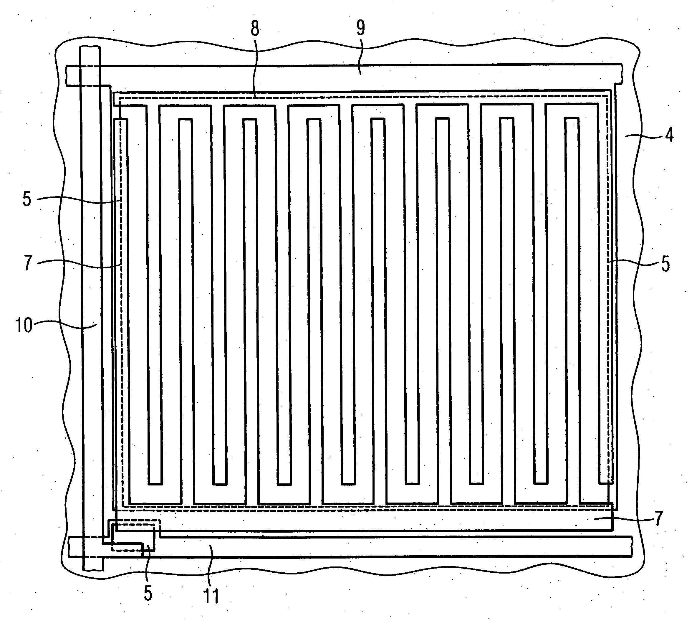
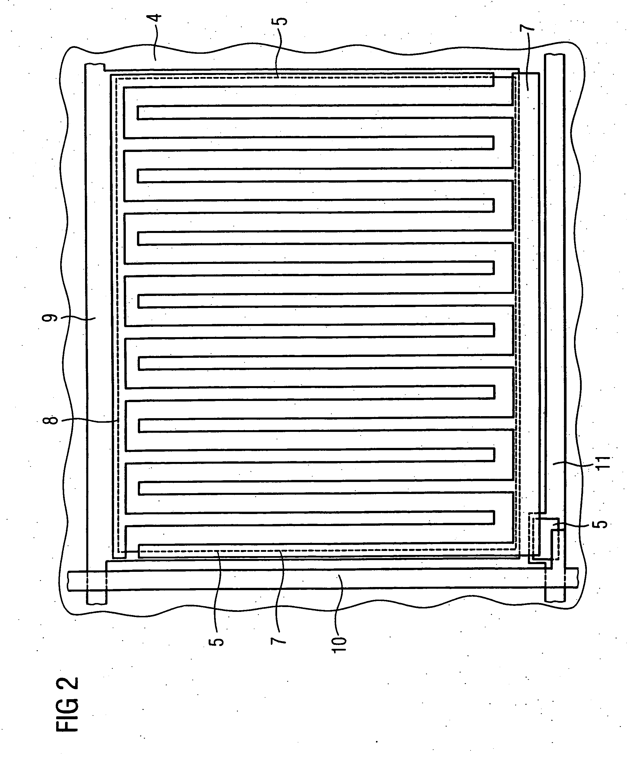
[0026] A photosensor element of a planar image detector is designated with 1 in FIGS. 1 and 2. Together with a number of further photosensor elements (which are not shown in FIGS. 1 and 2), the photosensor element 1 forms a planar image detector designed like a matrix.

[0027] The photosensor element 1 can be activated via at least one associated switching element 2 and has at least one storage element 3 with a predetermined capacity. The storage element 3 can be arranged above and / or below the photosensor element 1. In the shown exemplary embodiment, a storage element 3 is arranged only above the photosensor element 1.

[0028] The term “above” is defined with regard to the incidence direction of the rays. The radiation impinging on the photosensor element 1 thus first reaches the storage element 3 above the photosensor element 1 and then the photosensor element 1 itself.

[0029] In the shown exemplary embodiment the photosensor element 1 is fashioned as a phototransistor. In the embod...


PUM


Abstract

A planar image detector with a number of photosensor elements arranged like a matrix, the photosensor elements being activated by at least one associated switching element and respectively exhibiting at least one memory element with a predetermined capacity. A predetermined number of phototransistors each have a gate electrode that exhibits at least one gap in a gate metallization thereof and arranged between the source electrode and the drain electrode. The gap produces a space that is reduced in terms of field strength that can be realized simply in terms of production of such planar image detector.

Description

BACKGROUND OF THE INVENTION [0001] 1. Field of the Invention [0002] The invention concerns a planar detector for detecting a radiation image. [0003] 2. Description of the Prior Art [0004] A planar image detector with a sensor field composed of phototransistors arranged in a matrix is known from WO 03 / 073507 A2. The phototransistors are fashioned as thin film transistors (TFT) and can be individually activated by at least one associated switching element. Each thin film transistor has at least one storage element with a predetermined capacity, the memory element being arranged next to the thin film transistor. Due to its design, the planar image detector known from WO 03 / 073507 A2 necessitates a large total space requirement in order to achieve a predetermined active detector surface, or the active detector surface is correspondingly small given a predetermined total surface requirement. The known planar image detector thus exhibits a relatively disadvantageous ratio of active detect...

Claims


Application Information

Patent Timeline
IPC IPC(8): G01T1/20
CPCG01T1/2018G01T1/2006
Inventor KLAUSMANN, HAGENWITTMAN, GEORG
Owner SIEMENS HEALTHCARE GMBH
Why Eureka
Try Eureka