Method and apparatus for generating memory models and timing database

a technology of memory model and timing database, applied in the field of memory analysis, can solve the problems of long processing time and difficult process of generating timing model of customer memory for a particular mapping

Inactive Publication Date: 2007-06-14
BELL SEMICON LLC
View PDF18 Cites 5 Cited by
  • Summary
  • Abstract
  • Description
  • Claims
  • Application Information

AI Technical Summary

Problems solved by technology

Since the customer memory often can be mapped to the memory resources in a variety of different ways, the process of generating a timing model of the customer memory for a particular mapping can be come very difficult and may require design tools that process large amounts of data and have long processing times.

Method used


Image

  • Method and apparatus for generating memory models and timing database
  • Method and apparatus for generating memory models and timing database
  • Method and apparatus for generating memory models and timing database

Examples


Embodiment Construction

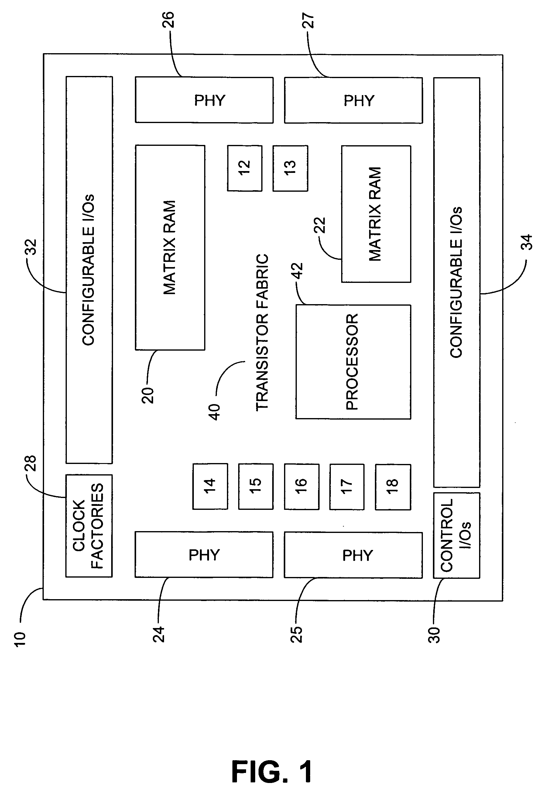
[0016] Integrated circuits are generally fabricated on a thin silicon wafer or substrate. Semiconductor devices and electrical interconnections that form the integrated circuit are conventionally made by building many mask layers on top of one another on the substrate. Each successive mask layer may have a pattern that is defined using a mask. A mask has a shape used for patterning features in a particular process step during fabrication. The mask layers are fabricated through a sequence of pattern definition steps using the masks, which are interspersed with other process steps such as oxidation, etching, doping and material deposition. When a mask layer is defined using a mask chosen or provided by a customer, the mask layer is programmed or customized.

[0017] The lowest, “base” layers include the active areas of the semiconductor devices, such as diffusion regions and gate oxide areas, and desired patterns of the polysilcon gate electrodes. One or more metal and insulating layers...


PUM


Abstract

A method and apparatus are provided for creating and using a memory timing database. A plurality of characterization memories are defined, which can be mapped to a memory resource. Each characterization memory has different memory parameters. A plurality of variants of tiling each characterization memory to the memory resource are also defined. Timing characteristics of each tiling variant of each characterization memory are stored in the memory timing database for the memory resource based on sets of input ramptimes and output loads.

Description

FIELD OF THE INVENTION [0001] The present disclosure relates to semiconductor integrated circuits. More particularly, the present disclosure relates to timing analysis of memories mapped to an integrated circuit layout pattern. BACKGROUND OF THE INVENTION [0002] In the design of integrated circuits, memory devices in a customer design are mapped to memory resources on an integrated circuit layout pattern. Depending on the technology, there may be a large number of different ways in which the memory can be mapped or “tiled” to the memory resources. [0003] It is customary for the integrated circuit manufacturer to provide the customer with various tools and models for assisting the customer in designing or customizing an integrated circuit for a particular application. Some integrated circuits have several different types of memory resources and can include large arrays of memory elements. Since the customer memory often can be mapped to the memory resources in a variety of different ...

Claims


Application Information

Patent Timeline
IPC IPC(8): G06F17/50
CPCG06F30/3312
Inventor ANDREEV, ALEXANDRENIKITIN, ANDREYSCEPANOVIC, RANKOVIKHLIANTSEV, IGOR
Owner BELL SEMICON LLC
Why Eureka
Try Eureka