Fluorene compound and organic light-emitting device
a fluorene compound and organic light-emitting technology, applied in the direction of discharge tube luminescnet screen, organic chemistry, natural mineral layered products, etc., can solve the problems of insufficient solution, degradation due, durability, etc., and achieve high efficiency and luminance, easy production, and high durability
- Summary
- Abstract
- Description
- Claims
- Application Information
AI Technical Summary
Benefits of technology
Problems solved by technology
Method used
Image
Examples
example 1
Synthesis of Exemplified Compound A-48
[0089]
[0090] In a 200 ml-three necked flask, 0.924 g (1.70 mmol) of compound-L-1, 0.957 g (3.40 mmol) of compound L-2, 0.65 g (6.80 mmol) of sodium tert-butoxide and 100 ml of xylene were placed. 34.4 mg (0.17 mmol) of tri-tert-butyl phosphine was added thereto under nitrogen atmosphere at room temperature with stirring, and then 48.9 mg (0.085 mmol) of palladium dibenzylideneacetone was added thereto. The mixture was heated to 125° C. and stirred at 125° C. for 3 hours. The organic layer was extracted with toluene, dried on anhydrous sodium sulfate and purified by using silica gel column (developing solvent: mixture of heptane and toluene) to obtain 0.920 g of compound A-48 (yellowish white crystal) (yield: 72.7%).
[0091] The following data of the obtained compound were confirmed.
[0092] M+: 743.5 (mass spectrometry)
[0093] m.p.: 323° C. (DSC: differential scanning calorimetry)
example 2
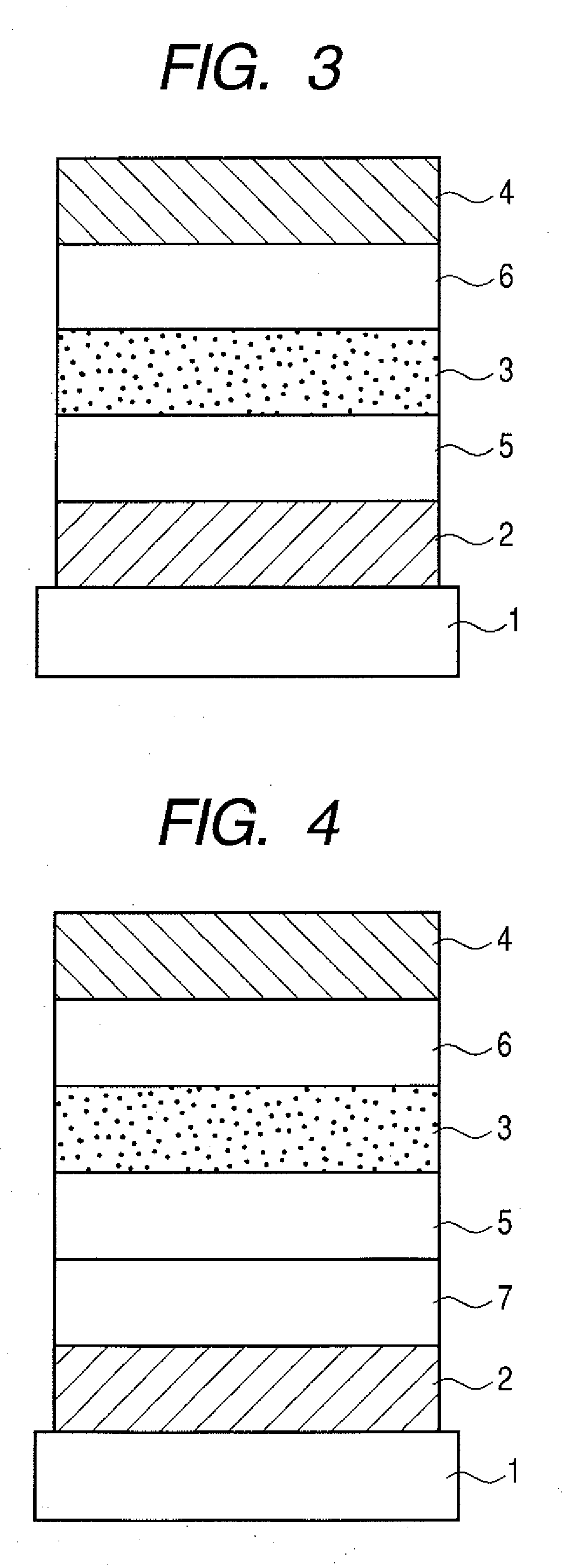
[0094] An organic light-emitting device having a structure as shown in FIG. 3 was produced by the following method.
[0095] On a glass substrate 1, a 120 nm-thick indium tin oxide (ITO) film as an anode 2 was formed by sputtering to prepare a transparent electroconductive support substrate. This was successively subjected to ultrasonic cleaning with acetone and isopropyl alcohol (IPA), in this order. The transparent electroconductive support substrate was then subjected to boiling cleaning with IPA and dried. Further it was subjected to UV / ozone cleaning, and was used as the transparent electroconductive support substrate.
[0096] The compound represented by the formula as shown below was used as a hole transport material, and a solution of the material in chloroform was prepared in a concentration of 0.1 wt %. This solution was added dropwise on the anode 2 of the transparent electroconductive support substrate, and spin coating was conducted at the beginning with rotation at 500 rpm...
examples 3 and 4
[0106] Organic light-emitting devices were produced and evaluated in the same manner as in example 1 except that as the first compound and the second compound, compounds as shown in Table 13 were used, respectively. Results are shown in Table 13 and Table 14.
TABLE 13FirstSecondAppliedcompoundcompoundvoltageLuminanceEfficiencyCentralExampleNo.No.(V)(cd / m2)(lm / W)wavelength (nm)3A-32C-5 435334.14604A-48C-11429913.5455
[0107]
TABLE 14Degradation of luminanceAfter 100 hoursExampleInitial (cd / m2)(cd / m2)329202290423401860
PUM
| Property | Measurement | Unit |
|---|---|---|
| thickness | aaaaa | aaaaa |
| deposition rate | aaaaa | aaaaa |
| deposition rate | aaaaa | aaaaa |
Abstract
Description
Claims
Application Information
 - R&D
- Intellectual Property
- Life Sciences
- Materials
- Tech Scout
- Unparalleled Data Quality
- Higher Quality Content
- 60% Fewer Hallucinations
Browse by: Latest US Patents, China's latest patents, Technical Efficacy Thesaurus, Application Domain, Technology Topic, Popular Technical Reports.
© 2025 PatSnap. All rights reserved.Legal|Privacy policy|Modern Slavery Act Transparency Statement|Sitemap|About US| Contact US: help@patsnap.com


