Semiconductor memory device

Inactive Publication Date: 2007-05-17
SOCIONEXT INC
View PDF8 Cites 3 Cited by
  • Summary
  • Abstract
  • Description
  • Claims
  • Application Information

AI Technical Summary

Benefits of technology

[0014] An object of the present invention is to prevent contention between a refresh operation and an access operation to prevent a malfunction in a semiconductor memory device which includes a multipurpose terminal receiving an address signal and a data signal and automatically performs refresh.
[0015] Another object of the present invention is to certainly receive an address signal supplied to a multipurpose terminal receiving an address signal and a data signal to prevent a malfunction of a semiconductor memory device.

Problems solved by technology

This causes contention between a refresh operation and an access operation, and thereby the pseudo-SRAM malfunctions.
Further, when an internal circuit of the semiconductor memory device is operated using the address signal with a short valid period, the timing margin of the internal circuit reduces, which makes a circuit design difficult.
If the timing margin reduces, the semiconductor memory device becomes more likely to be affected by a change in manufacturing condition, resulting in a decrease in yield.
If the erroneous address signal is selected, the semiconductor memory device malfunctions.
When a semiconductor memory device which includes the multipurpose terminal receiving the address signal and the data signal is newly designed, a design cost and a manufacturing cost of a photomask and so on are newly required.

Method used


Image

  • Semiconductor memory device
  • Semiconductor memory device
  • Semiconductor memory device

Examples


first embodiment

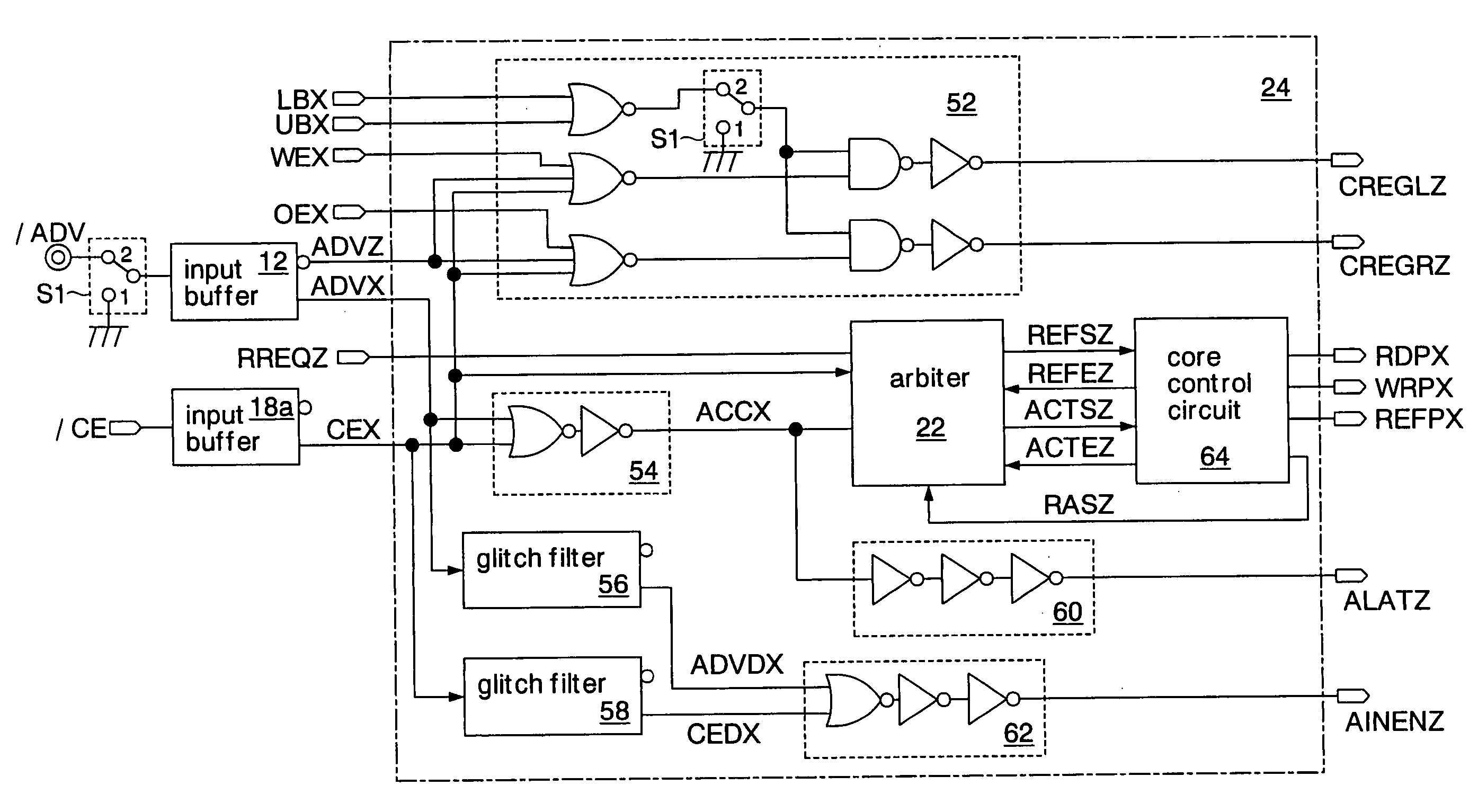
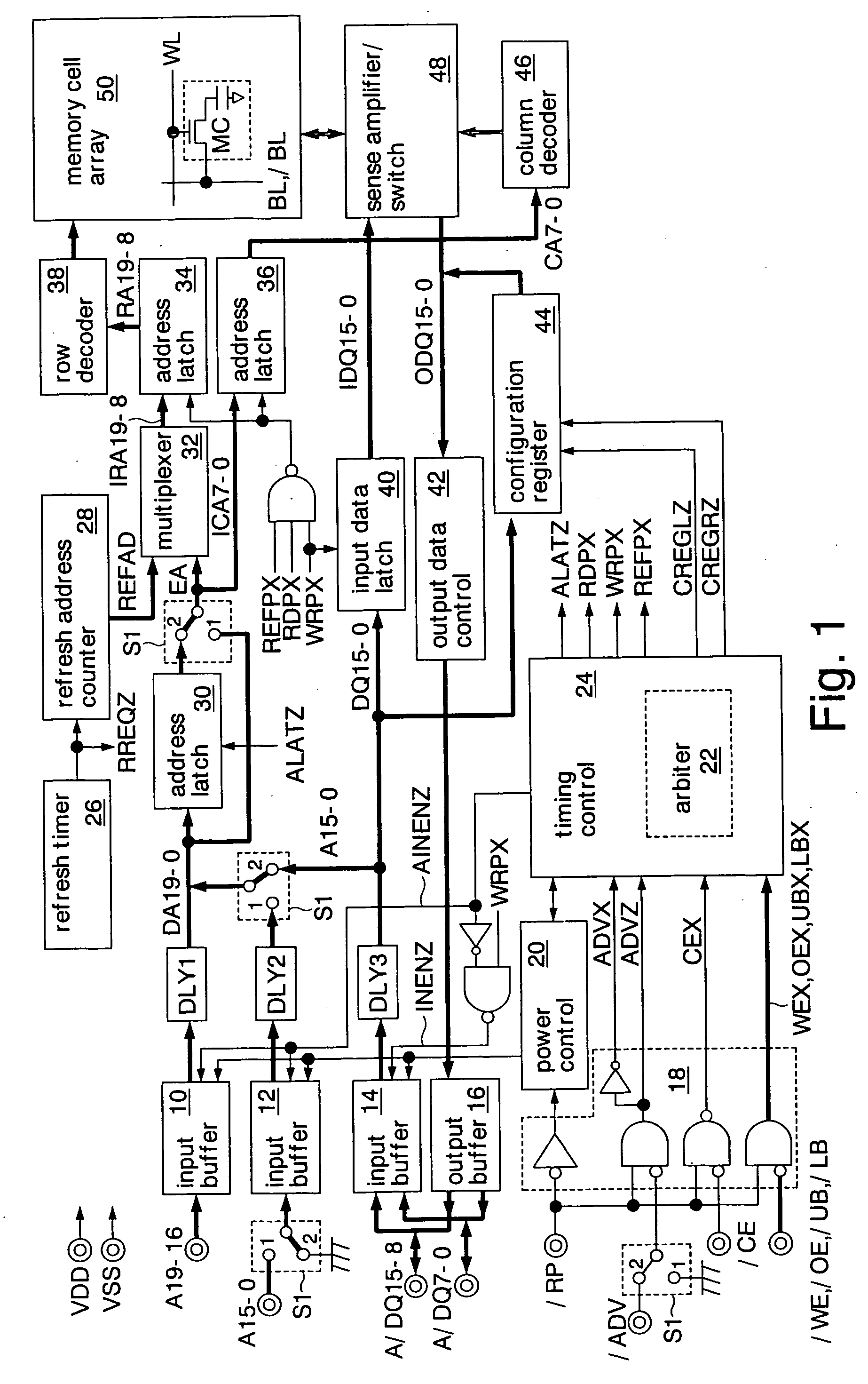
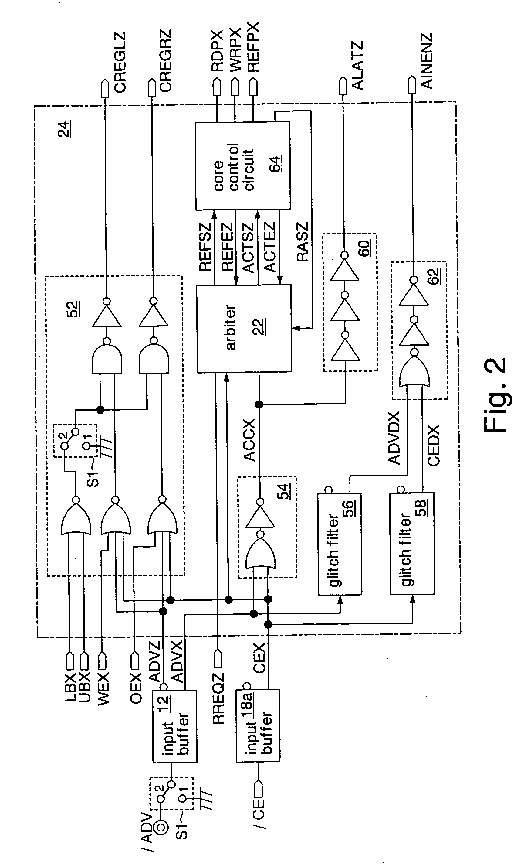
[0046]FIG. 1 shows a semiconductor memory device of the present invention. This semiconductor memory device is formed as a pseudo-SRAM on a silicon substrate using a CMOS process. The pseudo-SRAM is used, for example, for a work memory mounted in portable equipment such as a mobile phone.

[0047] The pseudo-SRAM includes input buffers 10, 12, 14, an output buffer 16, a command input circuit 18, a power control 20, a timing control 24 including an arbiter 22, delay circuits DLY1-3, a refresh timer (refresh request circuit) 26, a refresh address counter 28, a first address latch circuit 30, a multiplexer 32, second address latch circuits 34, 36, a row decoder 38, an input data latch circuit 40, an output data control 42, a configuration register 44, a column decoder 46, a sense amplifier / switch 48, a memory cell array 50, and plural specification setting units S1.

[0048] Each specification setting unit S1 is constituted of a conductive layer formed at a predetermined position on the sil...

second embodiment

[0134] In the above second embodiment, the example in which the specification setting unit S1 is constituted of the fuse is described. The present invention is not limited to this embodiment. For example, the specification setting unit S1 may be constituted using an electrically programmable memory cell such as an EPROM, an EEPROM, or an FeRAM instead of the fuse.

[0135] Although the present invention is described in detail above, the above embodiments and their modified examples are merely illustrative of the invention, and the present invention is not limited to these. It is understood that various modifications may be made without departing from the scope of the present invention.

[0136] By applying the present invention to a semiconductor memory device which includes an address valid terminal and automatically performs refresh, a malfunction of the semiconductor memory device due to contention between a refresh operation and an access operation can be prevented.


PUM


Abstract

A multipurpose terminal receives an address signal and a data signal. An address valid terminal receives an address valid signal indicating that a signal supplied to the multipurpose terminal is the address signal. An arbiter determines which of an external access request and an internal refresh request is given priority. The arbiter disables reception of the internal fresh request in response to a fact that both a chip enable signal and the address valid signal reach a valid level (an external access request). The arbiter enables the reception of the internal refresh request in response to completion of read or write operation. As a result, in a semiconductor memory device including the multipurpose terminal which receives the address signal and the data signal, contention between the read operation and the write operation, and a refresh operation which responds to the internal refresh request is prevented, which prevents a malfunction.

Description

CROSS REFERENCE TO RELATED APPLICATION [0001] This application is continuation application of International Application PCT / JP2004 / 010210, filed Jul. 16, 2004, and designation the U.S.BACKGROUND OF THE INVENTION [0002] 1. Field of the Invention [0003] The present invention relates to a semiconductor memory device which includes a multipurpose terminal receiving an address signal and a data signal and automatically refreshes a memory cell. [0004] 2. Description of the Related Art [0005] In recent years, a semiconductor memory called a pseudo-SRAM has been attracting attention. The pseudo-SRAM includes DRAM memory cells (dynamic memory cells) and operates as an SRAM by internally automatically performing a refresh operation of the memory cells. The dynamic memory cell is small in area. Therefore, the pseudo-SRAM with a low cost per bit and a large capacity can be developed. [0006] The pseudo-SRAM generates an internal refresh request to perform the refresh operation in a predetermined...

Claims


Application Information

Patent Timeline
IPC IPC(8): G11C7/00
CPCG11C7/1045G11C11/406G11C11/40603G11C11/40615G11C11/4076G11C11/34G11C11/401G11C11/408
Inventor TOMITA, HIROYOSHIYAMAGUCHI, SHUSAKU
Owner SOCIONEXT INC
Why Eureka
Try Eureka